


 产品分类
产品分类
Infineon 950 V CoolMOS P740W适配器解决方案
 116
116
 拍明
拍明
原标题:Infineon 950 V CoolMOS P740W适配器解决方案
infineon公司的950 V CoolMOS™ P7是适用于反激拓扑和功率因素修正(PFC)精心设计的器件,输出功率从10W到150W,是PFC和反激拓扑结构的理想之选.器件配有集成的齐纳二极管ESD保护.与同类竞争技术相比,具有同类产品最佳的效率和热性能,有高达0.2%的出色效率增益,并可将MOSFET温度降低高达5.2℃.主要用在从照明,智能电表,手机充电器,笔记本适配器到AUX电源和工业SMPS等各种应用.本文介绍了950 V CoolMOS™ P7主要特性和优势,以及采用950 V CoolMOS™ P7和ICE2QS03G 40W适配器评估板主要特性,电路图,材料清单和PCB设计图.
最新的950 V CoolMOS™ P7技术专注于低功率SMPS市场,旨在满足高压MOSFET领域不断增长的消费者需求。这款全新的P7系列产品适用于各种应用,从照明、智能电表、手机充电器、笔记本适配器到AUX电源和工业SMPS。新型950 V CoolMOS™ P7系列比其前代产品900 V CoolMOS™ C3提供高50 V的阻断电压,在效率、热性能和易用性方面表现出色。
与所有其他P7系列产品一样,950 V CoolMOS™ P7系列也配有集成的齐纳二极管ESD保护。该集成二极管显著提高了ESD稳健性,从而降低了与ESD相关的产量损失,并达到了极高的易用性水平。 CoolMOS™ P7采用一流的3 V VGS(th)和仅±0.5 V的偏差,使得它很容易驱动和实现设计导入。
凭借20多年的超级结技术经验,英飞凌推出具有一流DPAK导通电阻(RDS(on))的950 V
CoolMOS™ P7。此SMD器件的RDS(on)为450 mΩ - 与最接近的竞争产品相比,RDS(on)降低了60%以上。如此低的RDS(on)值可实现更高密度的设计,同时降低BOM和装配成本。
与竞争产品相比,950 V CoolMOS™ P7具有同类最佳的效率和热性能。在90 VAC下的 40 W适配器参考设计中即插即用,采用无缓冲器概念,与同类竞争技术相比,具有高达0.2%的出色效率增益,并可将MOSFET温度降低高达5.2℃。
950 V CoolMOS™ P7主要特性:
››一流的FOM RDS(on) Eoss;›
降低的Qg、Ciss和Coss
››一流的450 mΩ DPAK RDS(on)
››一流的3 V VGS(th)和最小的›
± 0.5 V VGS(th) 变化
››集成齐纳二极管ESD›
达到2级(HBM)保护
››一流的品质和可靠性
950 V CoolMOS™ P7主要优势:
››与CoolMOS™ C3相比,效率可提高1%,MOSFET温度可降低2℃至10℃
››实现更高功率密度设计、物料成本节省和更低的装配成本
››易于驱动和设计导入
››通过减少与ESD相关的故障来提高产量
›› 减少生产问题,减少退货
As already described, the 950 V CoolMOSTM P7 is a tailored technology for flyback topologies and Power Factor Correction (PFC). This chapter will introduce the main target market, which is applications from 10 W to 150 W. The difference between charger and adapter is the output voltage. Chargers typically operate at between 5 V and 12 V output voltage, and adapters use around 19 V. All these applications typically use flyback topologies. There are three main flyback structures that have the highest market share. First the Continuous Current Mode (CCM) flyback, second fixed-frequency DCM flyback, and finally QR flyback, which will be introduced in the next section. In addition the snubberlessflyback will also be described.
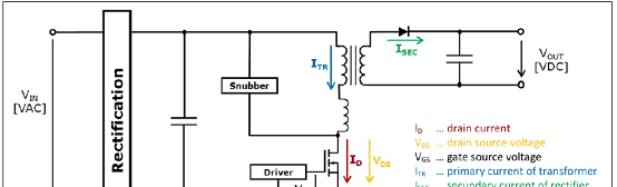
图1.简化的反激应用电路
采用950 V CoolMOS™ P7和ICE2QS03G 40W适配器评估板
The evaluation board described in this application note provides a test platform for the new 950 V CoolMOS™ P7 series of superjunction HV MOSFETs. The adapter uses the ICE2QS03G, a second-generation current mode control QR flyback controller and an IPA95R450P7 950 V CoolMOS™ P7 series power MOSFET. This application note is intended for those who have experience with flyback converter designs and will not cover the overall design process in depth, but it will cover specific design aspects for this controller and the 950 V CoolMOS™ P7 in charger and adapter applications. This design is done using a snubberlessflyback in order to improve the overall system efficiency while reducing the cost of the snubber network. This document will also show the overall benefits that the 950 V CoolMOS™ P7 presents for SMPS.
This 40 W adapter evaluation board (EVAL_40W_FLY_P7_950V) is intended to be a form, fit and function test platform for charger and adapter applications to show the operation of the 950 V CoolMOS™ P7 as well as the overall controller design. The evaluation board is designed around a QR flyback topology for improved switching losses that allows higher power density designs and lower radiated and conducted emissions. This board also employs a snubberlessflyback design in order to reduce the overall system costs while increasing system efficiency. This new efficiency can be used to give extra design flexibility to either further reduce system costs or increase power density. A 40 W universal input isolated flyback evaluation board with a 19 V output based on the ICE2QS03G controller and the 950 V CoolMOS™ P7 MOSFET is described in this application note, and test results are presented.
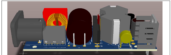
图2. 40W适配器(反激)评估板3D模型图
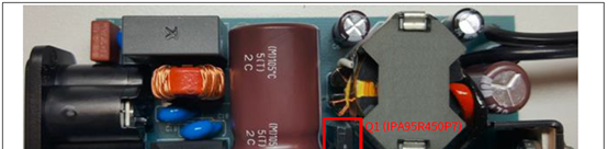
图3. 带TO-220 FullPAK封装的40W适配器(反激)评估板外形图(顶视)
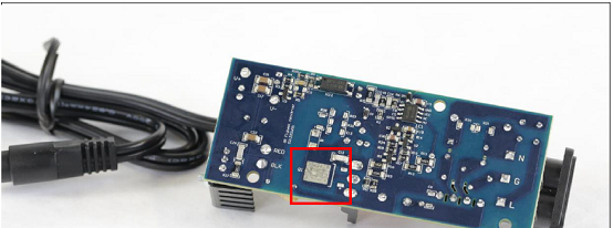
图4. 40W适配器(反激)评估板外形图(底视)(DPAK/SOT223封装)
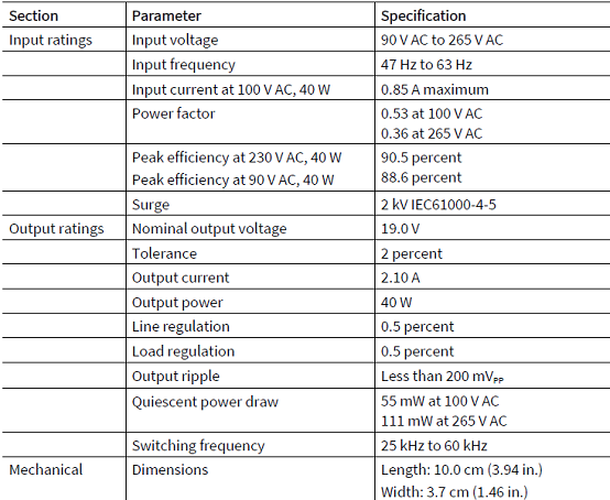
40W适配器(反激)评估板主要指标:
40W适配器(反激)评估板主要特性:
Fold-back point protection: For a QR flyback converter, the maximum possible output power is increased when a constant current limit value is used across the entire mains input voltage range. This is usually not desirable, as this will increase the cost of the transformer and output diode in the case of output over-power conditions. The internal fold-back protection is implemented to adjust the VCS voltage limit according to the bus voltage. Here, the input-line voltage is sensed using the current flowing out of the ZC pin, during the MOSFET on-time. As the result, the maximum current limit adjusts with the AC-line voltage.
VCC Over Voltage and Under Voltage Protection (OVP/UVP): During normal operation, the Vcc voltage is continuously monitored. When the Vcc voltage increases to VVCC OVP or Vcc voltage falls below the UVLO level VVCC off, the IC will enter auto-restart mode.
Over-load/open-loop protection: In the case of an open control loop, the feedback voltage is pulled up with an internal block. After a fixed blanking time, the IC enters auto-restart mode. In case of a secondary short-circuit or over-load, the regulation voltage VFB will also be pulled up, the same protection is applied and the IC will auto-restart.
Adjustable output OVP: During the off-time of the power switch, the voltage at the zero-crossing pin, ZC, is monitored for output over-voltage detection. If the voltage is higher than the preset threshold 3.7 V for a preset period of 100 μs, the IC is latched off.
Auto-restart for over-temperature protection: The IC has a built-in over-temperature protection function. When the controller’s temperature reaches 140℃, the IC will shut down the switch and enters auto-restart. This can protect the power MOSFET from overheating.
Short winding protection: The source current of the MOSFET is sensed via external resistors R15 and R16. If the voltage at the current sensing pin is higher than the preset threshold VCSSW of 1.68 V during the on-time of the power switch, the IC is latched off. This constitutes a short winding protection. To avoid an accidental latch-off, a spike blanking time of 190 ns is integrated into the output of the internal comparator.
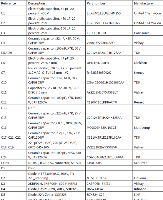
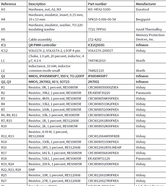
40W适配器(反激)评估板材料清单:
责任编辑:HanFeng
【免责声明】
1、本文内容、数据、图表等来源于网络引用或其他公开资料,版权归属原作者、原发表出处。若版权所有方对本文的引用持有异议,请联系拍明芯城(marketing@iczoom.com),本方将及时处理。
2、本文的引用仅供读者交流学习使用,不涉及商业目的。
3、本文内容仅代表作者观点,拍明芯城不对内容的准确性、可靠性或完整性提供明示或暗示的保证。读者阅读本文后做出的决定或行为,是基于自主意愿和独立判断做出的,请读者明确相关结果。
4、如需转载本方拥有版权的文章,请联系拍明芯城(marketing@iczoom.com)注明“转载原因”。未经允许私自转载拍明芯城将保留追究其法律责任的权利。
拍明芯城拥有对此声明的最终解释权。
相关资讯
:
基于MC33771主控芯片的新能源锂电池管理系统解决方案

AMIC110 32位Sitara ARM MCU开发方案

基于AMIC110多协议可编程工业通信处理器的32位Sitara ARM MCU开发方案

基于展讯SC9820超低成本LTE芯片平台的儿童智能手表解决方案

基于TI公司的AM437x双照相机参考设计

基于MTK6580芯片的W2智能手表解决方案


 2012- 2022 拍明芯城ICZOOM.com 版权所有 客服热线:400-693-8369 (9:00-18:00)


