基于ST L4984/L6699的400W高效率低待机功耗的AIO PC电源供应器解决方案
 484
484
 拍明
拍明
原标题:基于ST L4984及L6699的400W高效率低待机功耗的AIO PC电源供应器方案
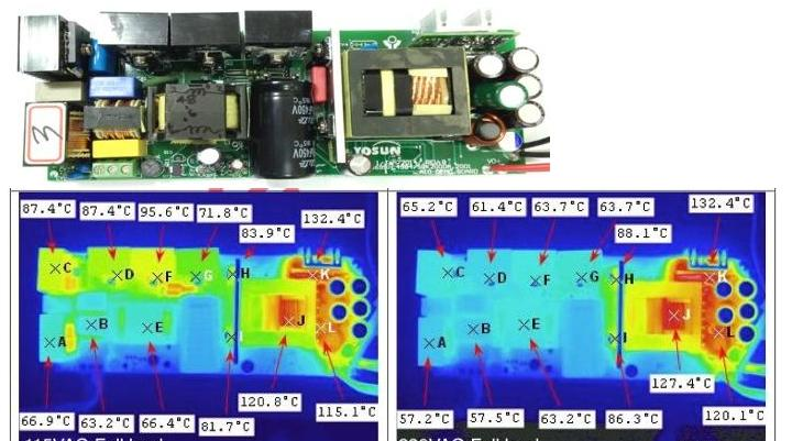
友尚制作400W-12V评估板是使用PFC加上LLC与同步整流架构,适用于高功率适配器和ATX电源的解决方案,在无/轻负载工作时功耗非常低,无需另外使用待机电源。
该应用有两级架构:使用L4984操作于CCM(连续导通模式)升压PFC控制器做功因修正,在供应给下一级的L6699器件做LLC谐振半桥转换器,提供12V稳压输出电压,可应用在ATX或类似应用,满足高效率和待机规定。
此评估板的主要重点是通过PFC和LLC控制器的Burst模式功能以及L6699器件的死区时间自我能调节,以提高轻载效率,由内部逻辑根据半桥节点转换时间进行监控,这可以使变压器磁化电感达到最大化,从而减轻轻载时的初级电流。
使用同步整流SRK2000/1器件,可获得正常负载运行时非常高的效率也可以使次级侧散热器的空间降低。
相关资料同步于ST网站 :
 PC电源供应器方案.png" alt="基于ST L4984/L6699的400W高效率低待机功耗的AIO PC电源供应器方案.png" style="width: 521px; height: 173px;" width="521" vspace="0" height="173" border="0"/>
场景应用图

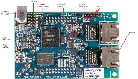
展示板照片
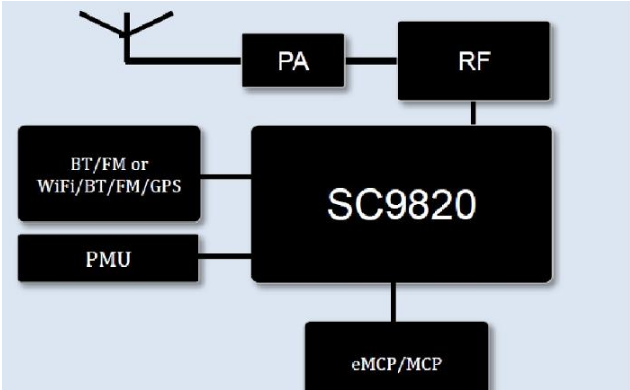
方案方块图
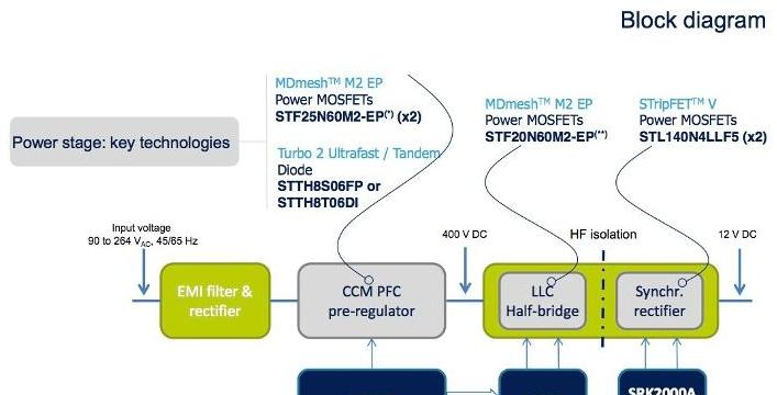
核心技术优势
Input: 90~264Vac交流电压
Output: 12V/400W直流电压
方案规格
1.低待机功耗,150mW以下。
2.高效率LLC架构与同步整流。
3.轻载高效率(0.5W待机功耗@0.25W抽载)。
技术文档
| 类别 | 标题 | 档案 |
|---|---|---|
| 硬件 | Gerber | |
| 硬件 | Power test report | |
| 硬件 | BOM |
【L4984D】
CCM PFC CONTROLLER
The L4984D is a current-mode PFC controller operating with line-modulated fixed-off-time (LM-FOT) control. A proprietary LM-FOT modulator allows fixed-frequency operation for boost PFC converters as long as they are operated in CCM (continuous conduction mode).
The chip comes in a 10-pin SO package and offers a low-cost solution for CCM-operated boost PFC pre-regulators in EN61000-3-2 and JEIDA-MITI compliant applications, in a power range that spans from few hundred W to 1 KW and above.
The highly linear multiplier includes a special circuit, able to reduce the crossover distortion of the AC input current, that allows wide-range-mains operation with a reasonably low THD, even over a large load range.
The output voltage is controlled by means of a voltage-mode error amplifier and an accurate (1% at Tj = 25 °C) internal voltage reference. Loop stability is optimized by the voltage feedforward function (1/V2correction), which in this IC uses a proprietary technique that also significantly improves line transient response in the case of mains drops and surges (“bi-directional”).
The device features low consumption and includes a disable function suitable for IC remote on/off. These features allow use in applications which also comply with the latest energy saving requirements (Blue Angel, ENERGY STAR, Energy 2000, etc.).
In addition to overvoltage protection able to keep the output voltage under control during transient conditions, the IC is also provided with protection against feedback loop failures or erroneous settings. Other onboard protection functions allow that brownout conditions and boost inductor saturation can be safely handled. Soft-start limits peak current and extends off-time to prevent flux runaway in the initial cycles.
The totem pole output stage, capable of 600 mA source and 800 mA sink current, is suitable for big MOSFETs or IGBT drive.
Key Features
Line-modulated fixed-off-time (LM-FOT) control of CCM-operated PFC pre-regulators
Proprietary LM-FOT modulator for nearly fixed-frequency operation
Proprietary multiplier design for minimum THD of AC input current
Fast “bi-directional” input voltage feedforward (1/V2correction)
Accurate adjustable output overvoltage protection
Protection against feedback loop failure (latched shutdown)
Inductor saturation protection
AC brownout detection
Digital leading-edge blanking on current sense
Soft-start
1% (at Tj = 25 °C) internal reference voltage
- 600 / + 800 mA totem pole gate driver with active pull-down during UVLO and voltage clamp
SSOP10 package
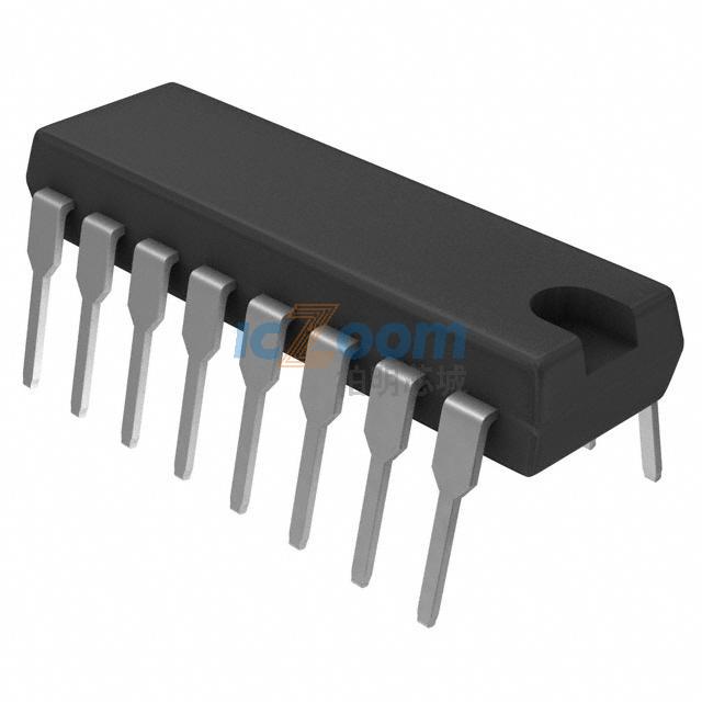
【L6699】
Enhanced high-voltage resonant controller
The L6699 is a double-ended controller specific to series-resonant half bridge topology. Both LLC and LCC configurations are supported. It provides symmetrical complementary duty cycle: the high-side switch and the low-side switch are driven ON/OFF 180° out-of-phase for exactly the same time. Output voltage regulation is obtained by modulating the operating frequency. The deadtime inserted between the turn-off of one switch and the turn-on of the other one is automatically adjusted to best fit the transition times of the half bridge midpoint. To drive the high-side switch with the bootstrap approach, the IC incorporates a high voltage floating structure able to withstand more than 600 V with a synchronous-driven high voltage DMOS that replaces the external fast-recovery bootstrap diode.
The IC enables the user to set the operating frequency range of the converter by means of a high-accuracy externally programmable oscillator.
At startup, in addition to the traditional frequency-shift soft-start (the switching frequency starts from a preset maximum value and then decays as far as the steady-state value determined by the control loop), a proprietary circuit controls the half bridge to prevent hard-switching from occurring in the initial cycles because of the unbalance in the V·s applied to the transformer.
At light load the IC can be forced to enter a controlled burst-mode operation that keeps the converter input consumption as low as possible.
IC protection functions include a current sense input for OCP with frequency shift and delayed shutdown with automatic restart. Fast shutdown with automatic restart occurs if this first-level protection cannot control the primary current. Additionally, the IC prevents the converter from working in or too close to the capacitive mode, to guarantee soft-switching. A latched disable input (DIS) can be used to implement OTP and/or OVP. The combination of these protection features offers the highest degree of safety.
Other functions include a not-latched active-low disable input with current hysteresis, useful for power sequencing or for brownout protection, and an interface with the PFC controller that enables the switching-off of the pre-regulator during fault conditions or during burst-mode operation.
Key Features
Symmetrical duty cycle, variable frequency control of resonant half bridge
Self-adjusting adaptive deadtime
High-accuracy oscillator
2-level OCP: frequency-shift and immediate shutdown
Interface with PFC controller
Anti-capacitive-mode protection
Burst-mode operation at light load
Input for brownout protection or power-on/off sequencing
“Safe-start” procedure prevents hard switching at startup
600 V rail compatible high-side gate driver with integrated bootstrap diode and high dv/dt immunity
-300/800 mA high-side and low-side gate drivers with UVLO pull-down
SO16N package
责任编辑:David
【免责声明】
1、本文内容、数据、图表等来源于网络引用或其他公开资料,版权归属原作者、原发表出处。若版权所有方对本文的引用持有异议,请联系拍明芯城(marketing@iczoom.com),本方将及时处理。
2、本文的引用仅供读者交流学习使用,不涉及商业目的。
3、本文内容仅代表作者观点,拍明芯城不对内容的准确性、可靠性或完整性提供明示或暗示的保证。读者阅读本文后做出的决定或行为,是基于自主意愿和独立判断做出的,请读者明确相关结果。
4、如需转载本方拥有版权的文章,请联系拍明芯城(marketing@iczoom.com)注明“转载原因”。未经允许私自转载拍明芯城将保留追究其法律责任的权利。
拍明芯城拥有对此声明的最终解释权。


 产品分类
产品分类




 2012- 2022 拍明芯城ICZOOM.com 版权所有 客服热线:400-693-8369 (9:00-18:00)


