基于ST STM32F334C8/STEVAL-ISA147V3/STM32F051K8的数字AC-DC电源供应器方案
 500
500
 拍明
拍明
原标题:基于ST STM32F334C8 Cortex M4 MCU的数字AC-DC电源供应器方案
AC-DC转换器设计用于从计算器适配器到服务器和电信系统的各种应用,要求在整个负载工作范围内以及通用电源输入电压范围内实现高效率。 鉴于对更高效,更小的适配器的需求,他们的设计变得越来越具有挑战性,并且已经研究了新的转换方法,而不是基于模拟IC的标准设计。 特别是,虽然标准方法基于使用升压型PFC和调节级,两者均使用模拟PWM调节器进行控制,但新的全数字方法依赖于使用微控制器来控制PFC和 DC-DC级。 这种方法越来越多地用于高密度,高效率的电力电子系统。
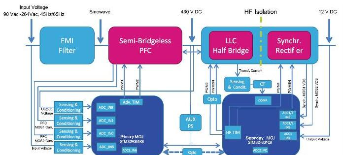
STEVAL-ISA147V3是一款数字开关模式AC-DC转换器,由两个功率级组成:一个由STM32F051K8控制的输入半桥功率因子校正器(SBPFC),一个由具有同步整流的LLC半桥实现的调节级(SR),由STM32F334C8微控制器控制。
这款500 W AC-DC转换器采用所谓的无桥PFC拓扑结构,无需二极管整流器级,具有传导损耗更低,效率更高的优势。与标准PFC相比,该选择还允许减少组件数量。
通常使用用于总线电压调节的外部电压回路和用于根据正弦波形形成电流的内部控制回路来控制输入级。外环调节电流基准,以维持调节的母线电压,与负载或输入电压变化无关。输出隔离和调节级采用半桥LLC拓扑结构实现,采用恒定工作周期和可变频率控制。
场景应用图
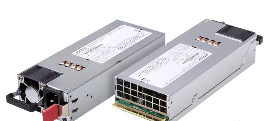
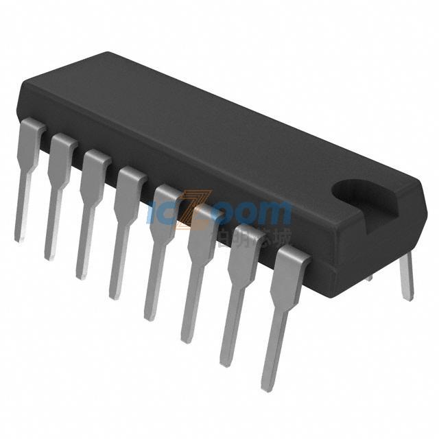
产品实体图
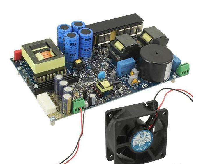
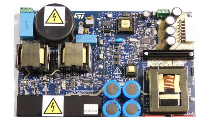
展示板照片
方案方块图
核心技术优势
1,高效率,低总谐波失真,保护机制
2,电力应用变得更加灵活和普遍
3,高输入功率因子可降低对电网的电力污染
4,智能模式管理和故障监控
5,实时监控和控制操作状态
6,降低系统和维护成本
方案规格
◾输入交流电压:90 V至264 V.
◾输入交流频率:45 Hz至65 Hz
◾标称功率:500 W
◾输出电压:12 V.
◾半无桥PFC级
◾DC-DC阶段:具有同步整流的谐振LLC
◾峰值效率:94%
◾PFC开关频率:60 kHz
◾DC-DC开关频率:80 kHz至115 kHz(以上突发模式)
◾HF变压器隔离电压:4 kV
◾冷却:自然对流高达300 W,强制冷却300 W以上
◾PFC控制:由STM32F051K8管理
◾LLC控制:由STM32F334C8管理
◾输入短路保护
◾输入欠压/过压保护
◾输入欠频/过频保护
◾DC总线欠压/过压保护
◾输出短路保护
◾输出欠压/过压保护
◾过温保护
◾符合RoHS标准
【STM32F334C8】
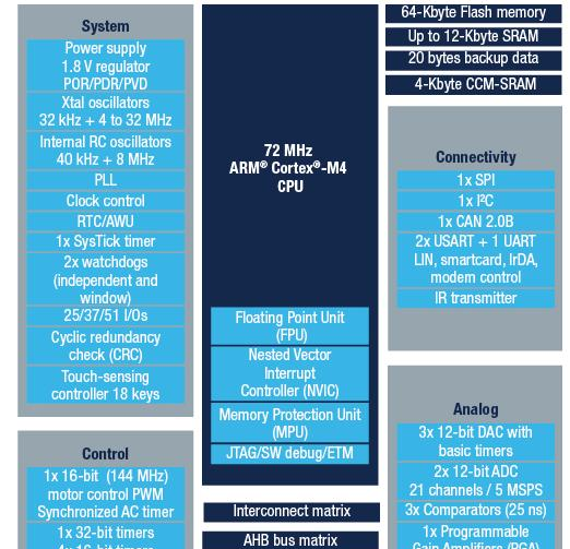
Mainstream Mixed signals MCUs ARM Cortex-M4 core with DSP and FPU, 64 Kbytes Flash, 72 MHz CPU, CCM, 12-bit ADC 5 MSPS, comparators, op-amp, hr timer
The STM32F334x4/6/8 family incorporates the high-performance Arm® Cortex®-M4 32-bit RISC core operating at up to 72 MHz frequency embedding a floating point unit (FPU), high-speed embedded memories (up to 64 Kbytes of Flash memory, up to 12 Kbytes of SRAM), and an extensive range of enhanced I/Os and peripherals connected to two APB buses.
The STM32F334x4/6/8 microcontrollers offer two fast 12-bit ADCs (5 Msps), up to three ultra-fast comparators, an operational amplifier, three DAC channels, a low-power RTC, one high-resolution timer, one general-purpose 32-bit timer, one timer dedicated to motor control, and four general-purpose 16-bit timers. They also feature standard and advanced communication interfaces: one I2C, one SPI, up to three USARTs and one CAN.
The STM32F334x4/6/8 family operates in the –40 to +85 °C and –40 to +105 °C temperature ranges from 2.0 to 3.6 V power supply. A comprehensive set of power-saving modes allow the design of low-power applications.
The STM32F334x4/6/8 family offers devices in 32, 48 and 64-pin packages.
Depending on the device chosen, different sets of peripherals are included.
主要特性
Core: Arm® Cortex®-M4 32-bit CPU with FPU (72 MHz max), single-cycle multiplication and HW division DSP instruction
Memories
Up to 64 Kbytes of Flash memory
Up to 12 Kbytes of SRAM with HW parity check
Routine booster: 4 Kbytes of SRAM on instruction and data bus with HW parity check (CCM)
CRC calculation unit
Reset and supply management
Low-power modes: Sleep, Stop, Standby
VDD,VDDA voltage range: 2.0 to 3.6 V
Power-on/Power-down reset (POR/PDR)
Programmable voltage detector (PVD)
VBAT supply for RTC and backup registers
Clock management
4 to 32 MHz crystal oscillator
32 kHz oscillator for RTC with calibration
Internal 8 MHz RC (up to 64 MHz with PLL option)
Internal 40 kHz oscillator
Up to 51 fast I/O ports, all mappable on external interrupt vectors, several 5 V-tolerant
Interconnect matrix
7-channel DMA controller
Up to two ADC 0.20 μs (up to 21 channels) with selectable resolution of 12/10/8/6 bits, 0 to 3.6 V conversion range, single-ended / differential mode, separate analog supply from 2.0 to 3.6 V
Temperature sensor
Up to three 12-bit DAC channels with analog supply from 2.4 V to 3.6 V
Three ultra-fast rail-to-rail analog comparators with analog supply from 2 to 3.6 V
One operational amplifiers that can be used in PGA mode, all terminals accessible with analog supply from 2.4 to 3.6 V
Up to 18 capacitive sensing channels supporting touchkeys, linear and rotary touch sensors
Up to 12 timers
HRTIM: 6 x16-bit counters, 217 ps resolution, 10 PWM, 5 fault inputs, 10 ext event input, 1 synchro. input,1 synchro. out
One 32-bit timer and one 16-bit timer with up to 4 IC/OC/PWM or pulse counter and quadrature (incremental) encoder input
One 16-bit 6-channel advanced-control timer, with up to 6 PWM channels, deadtime generation and emergency stop
One 16-bit timer with 2 IC/OCs, 1 OCN/PWM, deadtime generation, emergency stop
Two 16-bit timers with IC/OC/OCN/PWM, deadtime generation and emergency stop
Two watchdog timers (independent, window)
SysTick timer: 24-bit downcounter
Up to two 16-bit basic timers to drive DAC
Calendar RTC with alarm, periodic wakeup from Stop
Communication interfaces
CAN interface (2.0 B Active) and one SPI
One I2C with 20 mA current sink to support Fast mode plus, SMBus/PMBus
Up to 3 USARTs, one with ISO/IEC 7816 interface, LIN, IrDA, modem control
Debug mode: serial wire debug (SWD), JTAG
96-bit unique ID
All packages ECOPACK®2 compliant
STM32F334C8电路原理图
【STM32F334】
The STM32F3x4 product line is specifically addressing digital power conversion applications, such as D-SMPS, lighting, welding, inverters for solar systems and wireless chargers.
The main peripherals of the STM32F3x4 are:
High-resolution timer: 217ps, self-compensated versus power supply and temperature drift.
Ultra-fast comparator: 26ns from analog input to PWM shut-down
Ultra-fast 12-bit ADC 5Msps (0.2µs)
Operational amplifier with 5 built-in gain settings and 1% accuracy
The high resolution timer consists of a bank of 6 timers totaling:
10 PWM outputs (can be coupled by pairs)
10 external events inputs (Current limitation, Zero Voltage / Zero Current Detection…) and 5 fault inputs
The main features of the high resolution timers are:
217ps resolution available for all operating modes
Variable duty cycle, variable frequency, Transition mode,…
A number of features allows to unload the CPU
One DMA channel per timer
Built-in burst mode controller, topology specific modes: push-pull, resonant.
Numerous interconnects between timers to
Reset/Start adjacent timers
Set / Reset / Toggle other outputs
Transparent high-resolution implementation (equivalent to 4.6GHz timer) for easy programming
【STEVAL-ISA147V3】
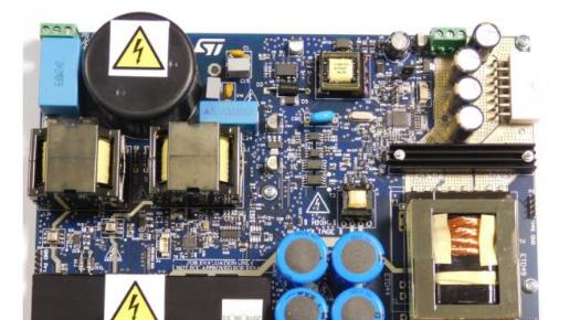
500 W fully digital AC-DC power supply (D-SMPS) based on STM32F334C8 microcontroller
The STEVAL-ISA147V3 is a digital switch mode AC-DC converter consisting of two power stages: an input semi-bridgeless power factor corrector (SBPFC) controlled by an STM32F051K8, and a regulation stage implemented with an LLC half bridge with synchronous rectification (SR), controlled by an STM32F334C8 microcontroller.
This 500 W AC-DC converter uses the so-called bridgeless PFC topology, with the advantage of lower conduction losses and higher efficiency by eliminating the need for a diode rectifier stage. This choice also allows a reduced component count compared to a standard PFC.
The input stage is typically controlled using an outer voltage loop for bus voltage regulation and an inner control loop to shape the current according to a sinusoidal waveform. The outer loop adjusts the current reference in order to maintain a regulated bus voltage, independent of load or input voltage variations. The output isolation and regulation stage is implemented using a half-bridge LLC topology, operating with constant duty cycle and variable frequency control.
Key Features
Input AC voltage: 90 V to 264 V
Input AC frequency: 45 Hz to 65 Hz
Nominal power: 500 W
Output voltage: 12 V
Semi-Bridgeless PFC stage
DC-DC stage: resonant LLC with synchronous rectification
Peak efficiency: 94%
PFC switching frequency: 60 kHz
DC-DC switching frequency: 80 kHz to 115 kHz (burst mode above)
HF transformer isolation voltage: 4 kV
Cooling: natural convection up to 300 W, forced cooling above 300 W
PFC control: managed by STM32F051K8
LLC control: managed by STM32F334C8
Input short-circuit protection
Input under/overvoltage protection
Input under/overfrequency protection
DC Bus under/overvoltage protection
Output short-circuit protection
Output under/overvoltage protection
Overtemperature protection
RoHS compliant
STEVAL-ISA147V3 IMAGE
【STM32F051K8】
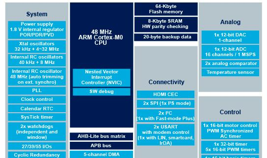
Mainstream ARM Cortex-M0 Access line MCU with 64 Kbytes Flash, 48 MHz CPU, motor control and CEC functions
The STM32F051xx microcontrollers incorporate the high-performance ARM®Cortex®-M0 32-bit RISC core operating at up to 48 MHz frequency, high-speed embedded memories (up to 64 Kbytes of Flash memory and 8 Kbytes of SRAM), and an extensive range of enhanced peripherals and I/Os. All devices offer standard communication interfaces (up to two I2Cs, up to two SPIs, one I2S, one HDMI CEC and up to two USARTs), one 12-bit ADC, one 12-bit DAC, six 16-bit timers, one 32-bit timer and an advanced-control PWM timer.
The STM32F051xx microcontrollers operate in the -40 to +85 °C and -40 to +105 °C temperature ranges, from a 2.0 to 3.6 V power supply. A comprehensive set of power-saving modes allows the design of low-power applications.
The STM32F051xx microcontrollers include devices in seven different packages ranging from 32 pins to 64 pins with a die form also available upon request. Depending on the device chosen, different sets of peripherals are included.
These features make the STM32F051xx microcontrollers suitable for a wide range of applications such as application control and user interfaces, hand-held equipment, A/V receivers and digital TV, PC peripherals, gaming and GPS platforms, industrial applications, PLCs, inverters, printers, scanners, alarm systems, video intercoms and HVACs.
Key Features
Core: ARM®32-bit Cortex®-M0 CPU, frequency up to 48 MHz
Memories
16 to 64 Kbytes of Flash memory
8 Kbytes of SRAM with HW parity checking
CRC calculation unit
Reset and power management
Digital and I/O supply: VDD= 2.0 V to 3.6 V
Analog supply: VDDA= from VDDto 3.6 V
Power-on/Power down reset (POR/PDR)
Programmable voltage detector (PVD)
Low power modes: Sleep, Stop, Standby
VBATsupply for RTC and backup registers
Clock management
4 to 32 MHz crystal oscillator
32 kHz oscillator for RTC with calibration
Internal 8 MHz RC with x6 PLL option
Internal 40 kHz RC oscillator
Up to 55 fast I/Os
All mappable on external interrupt vectors
Up to 36 I/Os with 5 V tolerant capability
5-channel DMA controller
One 12-bit, 1.0 μs ADC (up to 16 channels)
Conversion range: 0 to 3.6 V
Separate analog supply from 2.4 up to 3.6
One 12-bit DAC channel
Two fast low-power analog comparators with programmable input and output
Up to 18 capacitive sensing channels supporting touchkey, linear and rotary touch sensors
Up to 11 timers
One 16-bit 7-channel advanced-control timer for 6 channels PWM output, with deadtime generation and emergency stop
One 32-bit and one 16-bit timer, with up to 4 IC/OC, usable for IR control decoding
One 16-bit timer, with 2 IC/OC, 1 OCN, deadtime generation and emergency stop
Two 16-bit timers, each with IC/OC and OCN, deadtime generation, emergency stop and modulator gate for IR control
One 16-bit timer with 1 IC/OC
Independent and system watchdog timers
SysTick timer: 24-bit downcounter
One 16-bit basic timer to drive the DAC
Calendar RTC with alarm and periodic wakeup from Stop/Standby
Communication interfaces
Up to two I2C interfaces, one supporting Fast Mode Plus (1 Mbit/s) with 20 mA current sink, SMBus/PMBus and wakeup from Stop mode
Up to two USARTs supporting master synchronous SPI and modem control, one with ISO7816 interface, LIN, IrDA capability, auto baud rate detection and wakeup feature
Up to two SPIs (18 Mbit/s) with 4 to 16 programmable bit frame, one with I2S interface multiplexed
HDMI CEC interface, wakeup on header reception
Serial wire debug (SWD)
96-bit unique ID
All packages ECOPACK®2
STM32F051K8 CIRCUIT DIAGRAM
责任编辑:David
【免责声明】
1、本文内容、数据、图表等来源于网络引用或其他公开资料,版权归属原作者、原发表出处。若版权所有方对本文的引用持有异议,请联系拍明芯城(marketing@iczoom.com),本方将及时处理。
2、本文的引用仅供读者交流学习使用,不涉及商业目的。
3、本文内容仅代表作者观点,拍明芯城不对内容的准确性、可靠性或完整性提供明示或暗示的保证。读者阅读本文后做出的决定或行为,是基于自主意愿和独立判断做出的,请读者明确相关结果。
4、如需转载本方拥有版权的文章,请联系拍明芯城(marketing@iczoom.com)注明“转载原因”。未经允许私自转载拍明芯城将保留追究其法律责任的权利。
拍明芯城拥有对此声明的最终解释权。


 产品分类
产品分类




 2012- 2022 拍明芯城ICZOOM.com 版权所有 客服热线:400-693-8369 (9:00-18:00)


