基于ADI公司的AD9162数模转换器2.5 GHz宽带应用解决方案
 236
236
 拍明
拍明
原标题:ADI AD9162数模转换器2.5 GHz宽带应用解决方案
ADI公司的ad9162是16位12 GSPS数模转换器(DAC),动态范围高达-82 dBc SFDR和-167 dBm/Hz NSD,具有同类最佳的2.5 GHz带宽,支持超高清(UHD)和4K 电视,支持所有无线通信基础设施协议(WCDMA,LTE,LTE-A,点对点),有助于实现先进的多频段和多标准设计.主要用在宽带通信系统, DOCSIS 3.1电缆调制解调器终端系统(CMTS)/视频点播(VOD)/边沿正交幅度调制(EQAM),无线通信基础设施以及W-CDMA,LTE,LTE-A和点对点通信,仪器仪表,自动测试设备(ATE)与雷达和干扰发射器.本文介绍了AD9162产品亮点,主要特性和功能框图,以及评估板AD916x-FMCx-EBZ EVB主要特性,电路图和材料清单.
The AD9161/AD91621 are high performance, 11-bit/16-bit digital-to-analog converters (DACs) that supports data rates to 6 GSPS. The DAC core is based on a quad-switch architecture coupled with a 2× interpolator filter that enables an effective DAC update rate of up to 12 GSPS in some modes. The high dynamic range and bandwidth makes these DACs ideally suited for the most demanding high speed radio frequency (RF) DAC applications.
In baseband mode, wide bandwidth capability combines with high dynamic range to support DOCSIS 3.1 cable infrastructure compliance from the minimum of two carriers to full maximum spectrum of 1.794 GHz. A 2× interpolator filter (FIR85) enables the AD9161/AD9162 to be configured for lower data rates and converter clocking to reduce the overall system power and ease the filtering requirements. In Mix-Mode™ operation, the AD9161/ AD9162 can reconstruct RF carriers in the second and third Nyquist zones up to 7.5 GHz while still maintaining exceptional dynamic range. The output current can be programmed from 8 mA to 38.76 mA. The AD9161/AD9162 data interface consists of up to eight JESD204B serializer/deserializer (SERDES) lanes that are programmable in terms of lane speed and number of lanes to enable application flexibility.
A serial peripheral interface (SPI) can configure the AD9161/ AD9162 and monitor the status of all registers. The AD9161/ AD9162 are offered in an 165-ball, 8.0 mm × 8.0 mm, 0.5 mm pitch, CSP_BGA package and in an 169-ball, 11 mm × 11 mm, 0.8 mm pitch, CSP_BGA package, including a leaded ball option for the AD9162.
AD9162产品亮点:
1. High dynamic range and signal reconstruction bandwidth supports RF signal synthesis of up to 7.5 GHz.
2. Up to eight lanes JESD204B SERDES interface flexible in terms of number of lanes and lane speed.
3. Bandwidth and dynamic range to meet DOCSIS 3.1 compliance with margin.
AD9162主要特性:
DAC update rate up to 12 GSPS (minimum)
Direct RF synthesis at 6 GSPS (minimum)
DC to 2.5 GHz in baseband 1× bypass mode
DC to 6 GHz in 2× nonreturn-to-zero (NRZ) mode
1.5 GHz to 7.5 GHz in Mix-Mode
Bypassable interpolation (1× or bypass mode)
2×, 3×, 4×, 6×, 8×, 12×, 16×, 24×
Excellent dynamic performance
AD9162应用:
Broadband communications systems
DOCSIS 3.1 cable modem termination system (CMTS)/ video on demand (VOD)/edge quadrature amplitude modulation (EQAM)
Wireless communications infrastructure
W-CDMA, LTE, LTE-A, point to point
Instrumentation, automatic test equipment (ATE)
Radars and jammers

图1.AD9162功能框图
评估板AD916x-FMCx-EBZ EVB
The AD916x-FMCx-EBZ EVB connects to an ADS7-V1 or ADS7-V2 Pattern Generator to allow for quick evaluation of the AD916x, a high-speed, RF Digital to Analog converter (RF DAC). The ADS7 automatically formats the data and sends it to the AD916x EVB, simplifying evaluation of the device. The Evaluation Board (EVB) runs from the FMC power supply. The AD916x-FMCx-EBZ EVB can be driven by an external clock or the on-board clock, the ADF4355, as shown in Figure 1. There is a single pole, double throw (SPDT) switch on the board for selecting the clock source. Figure 2 is an image of the top side of the AD916x-FMCx-EBZ. The board includes a clock buffer, the AD9508, which provides the reference clock and SYSREF to the ADS7 and the SYSREF signal to DAC.
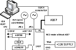
图2.评估板AD916x-FMCx-EBZ EVB框图和测试图

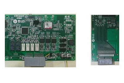
图3.评估板AD916x-FMCx-EBZ EVB外形图
责任编辑:HanFeng
【免责声明】
1、本文内容、数据、图表等来源于网络引用或其他公开资料,版权归属原作者、原发表出处。若版权所有方对本文的引用持有异议,请联系拍明芯城(marketing@iczoom.com),本方将及时处理。
2、本文的引用仅供读者交流学习使用,不涉及商业目的。
3、本文内容仅代表作者观点,拍明芯城不对内容的准确性、可靠性或完整性提供明示或暗示的保证。读者阅读本文后做出的决定或行为,是基于自主意愿和独立判断做出的,请读者明确相关结果。
4、如需转载本方拥有版权的文章,请联系拍明芯城(marketing@iczoom.com)注明“转载原因”。未经允许私自转载拍明芯城将保留追究其法律责任的权利。
拍明芯城拥有对此声明的最终解释权。


 产品分类
产品分类




 2012- 2022 拍明芯城ICZOOM.com 版权所有 客服热线:400-693-8369 (9:00-18:00)


