


 产品分类
产品分类
基于ADI公司的AD9172高性能取样12.6 GSPS双路16位DAC解决方案
 433
433
 拍明
拍明
原标题:ADI AD9172高性能取样12.6 GSPS双路16位DAC解决方案
ADI公司的AD9172是高性能双路取样高达12.6 GSPS的16位数模转换器(DAC),具有8路15 Gbps JESD204B数据输入端口,高性能片上DAC时钟倍频器和数字信号处理功能,支持单波段和多波段无线应用, 1.8GHz时的SFDR) <−80 dBc , IMD = −83 dBc, 12GSPS双路模式时的功耗为2.55W,主要应用在无线通信基础设备,多带基站无线电,微波/E波段回程传输系统,,工业仪表,自动测试设备(ATE)和雷达与干扰器.本文介绍了AD9172产品亮点和主要特性,功能框图,以及评估板AD9172-FMC-EBZ和电路图与材料清单.
The AD9172 is a high performance, dual, 16-bit digital-to-analogconverter (DAC) that supports DAC sample rates to 12.6 GSPS.The device features an 8-lane, 15 Gbps JESD204B data input port,a high performance, on-chip DAC clock multiplier, and digitalsignal processing capabilities targeted at single-band and multibanddirect to radio frequency (RF) wireless applications.
The AD9172 features three complex data input channels per RFDAC that are bypassable. Each data input channel includes aconfigurable gain stage, an interpolation filter, and a channelnumerically controlled oscillator (NCO) for flexible, multibandfrequency planning. The device supports up to a 1.5 GSPS complexdata rate per input channel and is capable of aggregating multiplecomplex input data streams up to a maximum complex data rateof 1.5 GSPS. Additionally, the AD9172 supports ultrawidebandwidth modes bypassing the channelizers to providemaximum data rates of up to 3.08 GSPS (with 16-bit resolution)and 4.1 GSPS (with 12-bit resolution).The AD9172 is available in a 144-ball BGA_ED package.
AD9172产品亮点:
1. Supports single-band and multiband wireless applicationswith three bypassable complex data input channels per RFDAC at a maximum complex input data rate of 1.5 GSPS.One independent NCO per input channel.
2. Ultrawide bandwidth channel bypass modes supporting upto 3 GSPS data rates with 16-bit resolution and 4 GSPSwith 12-bit resolution.
3. Low power dual converter decreases the amount of powerconsumption needed in high bandwidth and multichannelapplications.
AD9172主要特性:
Supports multiband wireless applications
3 bypassable, complex data input channels per RF DAC
1.54 GSPS maximum complex input data rate per inputchannel
1 independent NCO per input channel
Proprietary, low spurious and distortion design
2-tone intermodulation distortion (IMD) = −83 dBc at1.8 GHz, −7 dBFS/tone RF output
Spurious free dynamic range (SFDR) <−80 dBc at 1.8 GHz,−7 dBFS RF output
Flexible 8-lane, 15.4 Gbps JESD204B interface
Supports single-band and multiband use cases
Supports 12-bit high density mode for increased datathroughput
Multiple chip synchronization
Supports JESD204B Subclass 1
Selectable interpolation filter for a complete set of inputdata rates
1×, 2×, 3×, 4×, 6×, and 8× configurable data channelinterpolation
1×, 2×, 4×, 6×, 8×, and 12× configurable final interpolation
Final 48-bit NCO that operates at the DAC rate to supportfrequency synthesis up to 6 GHz
Transmit enable function allows extra power saving anddownstream circuitry protection
High performance, low noise PLL clock multiplier
Supports 12.6 GSPS DAC update rate
Observation ADC clock driver with selectable divide ratios
Low power
2.55 W at 12 GSPS, dual channel mode
10 mm × 10 mm, 144-ball BGA_ED with metal enhancedthermal lid, 0.80 mm pitch
AD9172应用:
Wireless communications infrastructure
Multiband base station radios
Microwave/E-band backhaul systems
Instrumentation, automatic test equipment (ATE)
Radars and jammers
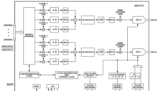
图1. AD9172功能框图
评估板AD9172-FMC-EBZ
The AD9172 evaluation board is an FMC form-factor board with FMC connector that complies to the Vita 57.1 standard. The FMC board uses a Mini-Circuits balun on the DAC output.
To operate the evaluation board, the user must attach the board to a compatible FMC carrier board, such as those provided by FPGA vendors. Analog Devices produces an FPGA carrier called the ADS7-V2, which serves as a digital pattern generator or data source as well as the power supply for the boards. The AD9172 board has an option to be powered from a lab power supply when used in a special NCO-only mode. This operation is described in more detail in the User ’ s Guide. The user must be able to observe the DAC output on a spectrum analyzer. A low noise clock source is provided on the evaluations boards, the HMC7044 clock synthesizer, and an option exists for the user to supply a low jitter external sine or square wave clock as a clock source instead. The evaluation board comes with software, called ACE, which allows the user to program the SPI port. Via the SPI port, the DUT (and clock circuitry) can be programmed into any of its various operating modes. It also comes with the DAC Software Suite which includes the DPGDownloader for vector generation, download, and transmission to the evaluation board when using the ADS7-V2.
Documentation and software updates for using High-Speed DAC Evaluation Boards are included in individual, self-extracting update files. The latest DPG Downloader software can be downloaded from here: High-Speed DAC Software Suite. The latest ACE software can be downloaded from here: Analysis | Control | Evaluation (ACE) Software. The plugins for this board can be downloaded from the plugin manager in the ACE software.
The AD9172 Evaluation Board Setup Guide provides details about how to set up the hardware and software for the evaluation kit. This guide explains how to setup the KCU-105 and the ADS8 and AD9172-FMC-EBZ. This evaluation kit will also support the Analog Devices ADS7 platform for lane rate configurations that are ≤12.5Gbps. The DPGDownloader software will be used to set up the data vectors and FPGA SERDES mode configuration for the KCU-105 platform, ADS8 or ADS7 and the ACE software (Analysis | Control | Evaluation) will be used to set up the AD9172 evaluation board, including the HMC7044 clock distribution chip on the board. The AD9172-FMC-EBZ evaluation board can be driven by an external direct clock with DAC PLL off or the on-board clock from HMC7044 with DAC PLL on. The reference clock of HMC7044 can be provided by the on-board 122.88MHz crystal or the external signal generator.
评估板套件包括:
The following items should be included in the evaluation kit (KCU-105 platform not included, purchased separately by the customer):
Interconnect Board (connects FX3 board to the KCU-105 FMC connector) with Cypress FX3 board (only needed if using the KCU-105)
USB2.0 Cable (connects FX3 board to USB port on a computer)
AD9172-FMC-EBZ Evaluation Board
Mini USB to USB Cable (connects mini USB port on evaluation board to USB port on a computer)
MicroSD card with preprogrammed FPGA image to be used with DPGDownloader software (not needed for ADS7 or ADS8)

图2.评估板AD9172-FMC-EBZ外形图
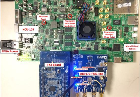
图3.评估板套件硬件连接图
详情请见:
![]() AD9172-FMC-EBZ RevC Gerber Files.zip
AD9172-FMC-EBZ RevC Gerber Files.zip
![]() AD9172-FMC-EBZ RevC Schematic.pdf
AD9172-FMC-EBZ RevC Schematic.pdf
责任编辑:HanFeng
【免责声明】
1、本文内容、数据、图表等来源于网络引用或其他公开资料,版权归属原作者、原发表出处。若版权所有方对本文的引用持有异议,请联系拍明芯城(marketing@iczoom.com),本方将及时处理。
2、本文的引用仅供读者交流学习使用,不涉及商业目的。
3、本文内容仅代表作者观点,拍明芯城不对内容的准确性、可靠性或完整性提供明示或暗示的保证。读者阅读本文后做出的决定或行为,是基于自主意愿和独立判断做出的,请读者明确相关结果。
4、如需转载本方拥有版权的文章,请联系拍明芯城(marketing@iczoom.com)注明“转载原因”。未经允许私自转载拍明芯城将保留追究其法律责任的权利。
拍明芯城拥有对此声明的最终解释权。
相关资讯
:
基于MC33771主控芯片的新能源锂电池管理系统解决方案

AMIC110 32位Sitara ARM MCU开发方案

基于AMIC110多协议可编程工业通信处理器的32位Sitara ARM MCU开发方案

基于展讯SC9820超低成本LTE芯片平台的儿童智能手表解决方案

基于TI公司的AM437x双照相机参考设计

基于MTK6580芯片的W2智能手表解决方案


 2012- 2022 拍明芯城ICZOOM.com 版权所有 客服热线:400-693-8369 (9:00-18:00)


