


 产品分类
产品分类
TI UCC28C43-Q1 BiCMOS低功耗电流模式PWM控制方案
 316
316
 拍明
拍明
原标题:TI UCC28C43-Q1 BiCMOS低功耗电流模式PWM控制方案
TI公司的ucc28C43-Q1是 BiCMOS高性能低功耗电流模式PWM控制器,满足AEC-Q100规范,工作温度-40⁰C到125⁰C,HBM分类为Level 2: ±2 kV, CDM分类Level C4B: 750 V,工作频率1MHz,峰值输出电流±1-A,主要用在汽车电源,混合和电动汽车,开关电源,DC/DC转换器,板安装电源模块.本文介绍了UCC28C43-Q1主要特性,功能框图, 汽车应用电路图,以及汽车应用40V-1kV输入反激参考设计TIDA-01505主要特性和系统指标,框图,电路图和材料清单.
The UCC28C4x-Q1 family devices are high performance current-mode PWM controllers. They are enhanced BiCMOS versions with pin-for-pin compatibility to the industry standard UC28C4x family PWM controllers.
Providing necessary features to control fixed frequency, peak current mode power supplies, this family offers several performance advantages. These devices offer high frequency operation up to 1 MHz with low start up and operating currents, thus minimizing start up loss and low operating power consumption for improved efficiency. The devices
also feature a fast current sense to output delay time of 35 ns, and a ±1-A peak output current capability with improved rise and fall times for driving large external MOSFETs directly.
The UCC28C4x-Q1 family is offered in the 8-pin SOIC (D) package.
UCC28C43-Q1主要特性:
1• AEC-Q100 Qualified with the Following Results:
– Device Temperature Grade 1:-40⁰C to 125⁰C
– Device HBM Classification Level 2: ±2 kV
– Device CDM Classification Level C4B: 750 V
• 1-MHz Operation
• 50-μA Standby Current, 100-μA Maximum
• Low Operating Current of 2.3 mA at 52 kHz
• Fast 35-ns Cycle-by-Cycle Over-Current Limiting
• ±1-A Peak Output Current
• Rail-to-Rail Output Swings With 25-ns Rise and 20-ns Fall Times
• ±1% Initial Trimmed 2.5-V Error Amplifier Reference
• Trimmed Oscillator Discharge Current
• New Undervoltage Lockout Versions
• Create a Custom Design Using the UCC28C4x-Q1 With the WEBENCH® Power Designer
UCC28C43-Q1应用:
• Automotive Power Supplies
• Hybrid and Electric Vehicles in Automotive
• Switch Mode Power Supplies
• DC-to-DC Converters
• Board Mount Power Modules
汽车应用40V-1kV输入反激参考设计TIDA-01505
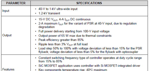
This power supply reference design for automotive auxiliary circuits generates a 15-V, 4-A output from a wide input range of 40 V to 1 kV and up to a 1.2-kV transient. The design fits ideally into an 800-V batterydriven hybrid-electric vehicle (HEV) or electric vehicle (EV) traction inverter system. The 40-V minimum input voltage supports the functional safety test for the regenerative braking from the traction motor. This reference design implements a silicon carbide (SiC) MOSFET with high blocking voltage and low gate charge to reduce switching losses. A non-isolated level shifter enables driving the SiC MOSFET from the Si MOSFET driver embedded in the flyback controller.
The board includes two flyback converter variants:
primary-side regulation (PSR) and optocoupler feedback to make comparisons and address different needs. The transformer design meets qualifications for Automotive AEC-Q200 Grade 1 with reinforced isolation.
This reference design is a 60-W power supply which enables an ultra-wide input range from a 40-V (minimum) to 1-kV (maximum) DC voltage targeted for use in 800-V battery systems. A primary feature of this design is that the converter can power up at the 40-V minimum input voltage, which allows support for the system safety test during the regenerative braking for traction inverters. This design is an auxiliary power supply solution that generates a 15-V output for the traction inverter subsystems. The design also
implements reinforced isolation for safety enhancement. The single-ended, flyback topology has been chosen due to its low cost, high isolation rating, and design simplicity. Moreover, the design includes two onboard converter variants, with optocoupler and primary side regulation (PSR) for performance comparisons.
Carefully consider the following criteria to fulfill the design requirements:
• Voltage blocking capability of the switching device –
Because of the high voltage, the Si MOSFET, which has a lower design margin for blocking voltage and high channel resistance, is not suitable. The design requires use of an SiC MOSFET with a higher blocking capability.
• Pulse-width modulated (PWM) switching duty cycle –
Support for such an ultra-wide input voltage range requires a controller that is able to operate within the corresponding, wide PWM duty-cycle range.
• Active start-up circuit –
The traditional, resistive start-up circuit causes high quiescent losses at high input voltage. This design implements an active start-up circuit for reduced leakage current.
• Noise coupling –
The high-voltage input and fast switching of the SiC MOSFET leads to high dv/dt switching nodes, which generates a large amount of noise and antenna loops. The essential switching nodes must be kept small and away from quiet areas to reduce the noise coupling.
• Safety clearance –
The distance between the high-voltage area at the primary side and low-voltage area at the secondary side must have enough clearance to comply with safety requirements. Reinforced isolations are normally imposed according to automotive safety requirements. The ground of the low-voltage side may be connected to a 12-V battery or vehicle chassis, which is touchable by the human body.
• Printed-circuit board (PCB) clearance and high-voltage components selection –
The PCB clearance must be carefully designed to avoid electrical breakdown failure. Carefully select components that tolerate high voltages to properly handle the high-voltage stress.
This reference design is capable of powering up from a 40-V minimum input voltage for the purpose of enabling engineers to work safely and allow them to test the regenerative braking mechanism.
Regenerative braking utilizes the same insulated-gate bipolar transistor (IGBT)-based traction inverter to force the power flow in the reverse direction from the motor and send the power back to the battery. The IGBTs are controlled in a different algorithm to regulate the DC output from AC. Regenerative braking technology funnels the energy created by the braking process back into the system in the form of charging the battery for further use. Typically, in a regenerative braking system, the energy loss from the braking process transfers to the generator from the rotating axel before transferring to the battery, thus saving energy.
参考设计TIDA-01505主要特性:
• 40-V to 1-kV input, 15-V Output Flyback Auxiliary Power Supply With Output Power up to 60 W
• Regulated 15 V With Active Start-Up Circuit for Reduced Standby Power
• Extendable to Higher Voltage and Higher Power Range to Utilize High-Voltage Capability of SiC MOSFET
• Automotive Grade 1 Qualified Transformer With Reinforced Isolation (Qualified With 5.7-kV High- Pot Test)
• Two Converter Variants With PSR and Optocoupler Feedback Included on Board
• Constant Switching Frequency Type of Controller With Maximum Switching Frequency of 1 MHz and Duty Cycle Range From 0% to 96%
参考设计TIDA-01505应用:
• HEV/EV Traction Inverter
• HEV/EV On Board Charger
• Electronic Control Units
• HEV/EV DC/DC Converters
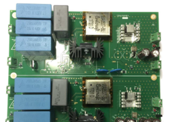
图. 参考设计TIDA-01505外形图
主要系统指标:
详情请见:
责任编辑:HanFeng
【免责声明】
1、本文内容、数据、图表等来源于网络引用或其他公开资料,版权归属原作者、原发表出处。若版权所有方对本文的引用持有异议,请联系拍明芯城(marketing@iczoom.com),本方将及时处理。
2、本文的引用仅供读者交流学习使用,不涉及商业目的。
3、本文内容仅代表作者观点,拍明芯城不对内容的准确性、可靠性或完整性提供明示或暗示的保证。读者阅读本文后做出的决定或行为,是基于自主意愿和独立判断做出的,请读者明确相关结果。
4、如需转载本方拥有版权的文章,请联系拍明芯城(marketing@iczoom.com)注明“转载原因”。未经允许私自转载拍明芯城将保留追究其法律责任的权利。
拍明芯城拥有对此声明的最终解释权。
相关资讯
:
基于MC33771主控芯片的新能源锂电池管理系统解决方案

AMIC110 32位Sitara ARM MCU开发方案

基于AMIC110多协议可编程工业通信处理器的32位Sitara ARM MCU开发方案

基于展讯SC9820超低成本LTE芯片平台的儿童智能手表解决方案

基于TI公司的AM437x双照相机参考设计

基于MTK6580芯片的W2智能手表解决方案


 2012- 2022 拍明芯城ICZOOM.com 版权所有 客服热线:400-693-8369 (9:00-18:00)


