


 产品分类
产品分类
基于On Semi公司的RSL10多协议无线系统级芯片(SoC)开发方案
 252
252
 拍明
拍明
原标题:On Semi RSL10多协议无线系统级芯片(SoC)开发方案
On Semi公司的RSL10是超低功耗的多协议无线系统级芯片(SoC),采用ARMR CortexR−M3处理器(48MHz)和LPDSP32 DSP核(音频CODEC),支持蓝牙5.0低功耗技术和2.4GHz多协议堆栈,Rx接收灵敏度-94dBm,数据速率62.5-2000kbps,发送功率-17到+6dBm,工作电压1.1-3.3V,主要用在可穿戴,物联网(IoT),无线使能低压设备和汽车电子.本文介绍了RSL10主要特性,框图和架构图,应用电路图,以及IoT IDK BLERSL10评估板BLE-IOT-GEVB主要特性,电路图,材料清单和PCB设计图.
RSL10 is an ultra−low−power, highly flexible multi−protocol2.4 GHz radio specifically designed for use in high−performancewearable and medical applications. With its ARMR CortexR−M3Processor and LPDSP32 DSP core, RSL10 supports Bluetooth lowenergy technology and 2.4 GHz proprietary protocol stacks, withoutsacrificing power consumption.
RSL10主要特性:
• Rx Sensitivity (Bluetooth Low Energy Mode, 1 Mbps): −94 dBm
• Data Rate: 62.5 to 2000 kbps
• Transmitting Power: −17 to +6 dBm
• Peak Rx Current = 5.6 mA (1.25 V VBAT)
• Peak Rx Current = 3.0 mA (3 V VBAT)
• Peak Tx Current (0 dBm) = 8.9 mA (1.25 V VBAT)
• Peak Tx Current (0 dBm) = 4.6 mA (3 V VBAT)
• Bluetooth 5 Certified with LE 2M PHY Support
• ARM Cortex−M3 processor clocked up to 48 MHz
• LPDSP32 for Audio Codec
• Supply Voltage Range: 1.1 − 3.3 V
• Current Consumption (1.25 V VBAT):
♦ Deep Sleep, IO wake−up: 50 nA
♦ Deep Sleep, 8 kB RAM retention: 300 nA
♦ Audio Streaming at 7 kHz audio BW: 1.8 mA RX, 1.8 mA TX
• Current Consumption (3 V VBAT):
♦ Deep Sleep, IO wake−up: 25 nA
♦ Deep Sleep, 8 kB RAM retention: 100 nA
♦ Audio Streaming at 7 kHz audio BW: 0.9 mA RX, 0.9 mA TX
• 384 kB of flash memory
• Highly−integrated System−on−Chip (SoC)
• Supports FOTA (Firmware Over−The−Air) updates
• ARM Cortex−M3 Processor: A 32−bit core forreal−time applications, specifically developed to enablehigh−performance low−cost platforms for a broad rangeof low−power applications.
• LPDSP32: A 32−bit Dual Harvard DSP core thatefficiently supports audio codecs required for wirelessaudio communication. Various codecs are available tocustomers through libraries that are included inRSL10’s development tools.
• Radio frequency Front−End: Based on a 2.4 GHz RFtransceiver, the RFFE implements the physical layer ofthe Bluetooth low energy technology standard and other
proprietary or custom protocols.
• Protocol Baseband Hardware: Bluetooth 5 certifiedand includes support for a 2 Mbps RF link and customprotocol options. The RSL10 baseband stack issupplemented by support structures that enableimplementation of ON Semiconductor and customerdesigned custom protocols.
• Highly−Integrated SoC: The dual−core architecture iscomplemented by high−efficiency power managementunits, oscillators, flash and RAM memories, a DMA
controller, along with a full complement of peripheralsand interfaces.
• Deep Sleep Mode: RSL10 can be put into a DeepSleep Mode when no operations are required. VariousDeep Sleep Mode configurations are available,including:
♦ “IO wake−up” configuration. The powerconsumption in deep sleep mode is 50 nA (1.25 VVBAT).
♦ Embedded 32 kHz oscillator running with interruptsfrom timer or external pin. The total current drain is90 nA (1.25 V VBAT).
♦ As above with 8 kB RAM data retention. The totalcurrent drain is 300 nA (1.25 V VBAT).
♦ With the exception of IO wake up onlyconfiguration, the on−chip buck converter can alsobe enabled to reduce current consumption in DeepSleep Mode (at higher VBAT voltages).
• Standby Mode: Can be used to reduce the averagepower consumption for off−duty cycle operation,ranging typically from a few ms to a few hundreds ofms.The typical chip power consumption is 30 _A inStandby Mode.
• Multi−Protocol Support: Using the flexibilityprovided by LPDSP32, the ARM Cortex−M3 processor,and the RF front−end; proprietary protocols and othercustom protocols are supported.
• Flexible Supply Voltage: RSL10 integrates high−efficiency power regulators and has a VBAT range of1.1 to 3.3 V.
• Highly Configurable Interfaces: I2C, UART, two SPIinterfaces, PCM interface, multiple GPIOs. It alsosupports a digital microphone interface and an outputdriver.
• The Asynchronous Sample Rate Converter (ASRC)Block and Audio Sink Clock Blocks Provides a meansof synchronizing the audio sample rate between anaudio source and an audio sink. The audio sink clockalso provides a high accuracy mechanism to measure aninput clock used for the RTC or protocol timing.
• Flexible Clocking Scheme: RSL10 must be clockedfrom the XTAL/PLL of the radio front−end at 48 MHzwhen transmitting or receiving RF traffic. When RSL10is not transmitting/receiving RF traffic, it can run offthe 48 MHz XTAL, the internal RC oscillators, the32 kHz oscillator, or an external clock. A lowfrequency RTC clock at 32 kHz can also be used inDeep Sleep Mode. It can be sourced from either theinternal XTAL, the RC oscillator, or a digital input pad.
• Diverse Memory Architecture: 76 kB of SRAMprogram memory and 88 kB of SRAM data memoryare available. A total of 384 kB of flash is available tostore the Bluetooth stack and other applications. TheARM Cortex−M3 processor can execute from SRAMand/or flash.
• IP Protection Feature: Ensures that the customer’sflash contents cannot be copied by a third party. Itprevents any core or memory from being accessedexternally after the chip has booted.
• Ultra−Low Power Consumption ApplicationExamples:
♦ Audio Signal Streaming: IDD <1.8 mA @ VBAT1.25 V in Rx Mode for receiving, decoding andsending an 7 kHz bandwidth audio signal to the SPIinterface using a proprietary custom audio protocolfrom ON Semiconductor.
♦ Low Duty Cycle Advertising: IDD 1.3 _A foradvertising at all three channels at 5 second intervals@ VBAT 3 V, DCDC converter enabled.
• Development Tools: Includes development hardwareand the standard Eclipse−based and other IntegratedDevelopment Environment (IDE) components for theARM Cortex−M3 processor. The LPDSP32 code can bedeveloped using the Synopsys development tools,which are available by request.
• RoHS Compliant device
RSL10应用:
Wearables
IoT Applications
Wireless-Enabled Low-Voltage Devices (1.2 V, 1.5 V Batteries Without DC/DC Converter)
Automotive
RSL10终端产品:
Fitness Trackers/Activity Monitors
Smart Watches
Hearing Aids/Hearables
Heart Rate Monitors
Blood Glucose Monitors (BGM)
Continuous Glucose Monitors (CGM)
Pulse Oximeters
Appliances (e.g., A/C, fans, etc.)
Smart Locks
Lighting Applications
Automotive Applications (Qualification Ready Q2/18)

图1.RSL10框图

图2. RSL10架构图

图3. RSL10 3.3V应用框图

图4. RSL101.25V应用框图
IoT IDK BLERSL10评估板BLE-IOT-GEVB
The BLE-IOT-GEVB evaluation board adds Bluetooth 5 and BLE functionality to the IoTDevelopment Kit (IDK).

图5.评估板BLE-IOT-GEVB外形图
评估板BLE-IOT-GEVB主要特性:
Ultra-low power, Bluetooth 5 certified SoC – RSL10 (Cortex M3, LPDSP)
Connects to IDK through Arduino style connectors
Combine with sensors and actuators on the IDK to prototype complex use cases
Integrated PCB antenna
Antenna Matching and Filtering Network

图6.评估板BLE-IOT-GEVB电路图(1)

图7.评估板BLE-IOT-GEVB电路图(2)

图8.评估板BLE-IOT-GEVB电路图(3)

图9.评估板BLE-IOT-GEVB电路图(4)
评估板BLE-IOT-GEVB材料清单:


图10.评估板BLE-IOT-GEVB PVCB设计图(1)

图11.评估板BLE-IOT-GEVB PVCB设计图(2)

图12.评估板BLE-IOT-GEVB PVCB设计图(3)

图13.评估板BLE-IOT-GEVB PVCB设计图(4)

图14.评估板BLE-IOT-GEVB PVCB设计图(5)

图15.评估板BLE-IOT-GEVB PVCB设计图(6)

图16.评估板BLE-IOT-GEVB PVCB设计图(7)
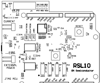
图17.评估板BLE-IOT-GEVB PVCB设计图(8)

图18.评估板BLE-IOT-GEVB PVCB设计图(9)

图19.评估板BLE-IOT-GEVB PVCB设计图(10)

图20.评估板BLE-IOT-GEVB PVCB设计图(11)

图21.评估板BLE-IOT-GEVB PVCB设计图(12)

图22.评估板BLE-IOT-GEVB PVCB设计图(13)
详情请见:
责任编辑:Davia
【免责声明】
1、本文内容、数据、图表等来源于网络引用或其他公开资料,版权归属原作者、原发表出处。若版权所有方对本文的引用持有异议,请联系拍明芯城(marketing@iczoom.com),本方将及时处理。
2、本文的引用仅供读者交流学习使用,不涉及商业目的。
3、本文内容仅代表作者观点,拍明芯城不对内容的准确性、可靠性或完整性提供明示或暗示的保证。读者阅读本文后做出的决定或行为,是基于自主意愿和独立判断做出的,请读者明确相关结果。
4、如需转载本方拥有版权的文章,请联系拍明芯城(marketing@iczoom.com)注明“转载原因”。未经允许私自转载拍明芯城将保留追究其法律责任的权利。
拍明芯城拥有对此声明的最终解释权。
相关资讯
:
基于MC33771主控芯片的新能源锂电池管理系统解决方案

AMIC110 32位Sitara ARM MCU开发方案

基于AMIC110多协议可编程工业通信处理器的32位Sitara ARM MCU开发方案

基于展讯SC9820超低成本LTE芯片平台的儿童智能手表解决方案

基于TI公司的AM437x双照相机参考设计

基于MTK6580芯片的W2智能手表解决方案


 2012- 2022 拍明芯城ICZOOM.com 版权所有 客服热线:400-693-8369 (9:00-18:00)


