


 产品分类
产品分类
ADI ADA4254零飘移高压低功耗可编增益仪表放大器解决方案
 134
134
 拍明
拍明
原标题:ADI ADA4254零飘移高压低功耗可编增益仪表放大器解决方案
ADI公司的ADA4254是零飘移高压低功耗可编增益仪表放大器(PGIA),具有12二进制加权增益,从1/16V/V到128V/V,具有三个可选增益1V/V,1.25V/V和1.35V/V,一共有36种可设增益.而ADA4254的功耗仅仅为22mW,特别适合于需要精密鲁棒和低功耗的工业系统.零飘移放大器拓扑采用自校准DC误差和低频1/f噪音,在整个温度范围内具有极好的DC精度,从而最大化动态范围,在许多应用中大大降低了校准要求.输入的复接器对放大器高阻抗输入提供±60 V保护,同时能在两个输入源中进行切换.此外,电磁干扰(EMI)滤波器阻隔了放大器敏感输入的RF噪音. ADA4254的各种安全特性检测内部和外部的故障.七个通用兵输入/输出(GPIO)引脚可配置成特别的功能,激励电流输出可用来偏压传感器如电阻型温度检测器(RTD).工作温度−40℃到 +105℃,采用紧凑的5mmx5mm28引脚LFCSP和24引脚TSSOP封装.工作电压±5 V 到 ±28 V.主要用在通用过程控制前端,数据采集系统和测试测量系统.本文介绍了ADA4254主要特性,简化功能框图和可编增益仪表放大器拓扑图,多种应用电路图,以及评估板ADA4254RU-EBZ主要特性,电路图和材料清单.
The ADA4254 is a zero drift, high voltage, low power programmable gain instrumentation amplifier (PGIA) designed for process control and industrial applications. The ADA4254 features 12 binary weighted gains ranging from 1/16 V/V to 128 V/V and three scaling gain options of 1 V/V, 1.25 V/V, and 1.375 V/V, resulting in 36 possible gain settings. The power consumption of the ADA4254 is a mere 22 mW, making the device an excellent choice for industrial systems that demand precision, robustness, and low power.
The zero drift amplifier topology of the ADA4254 self calibrates dc errors and low frequency 1/f noise, achieving excellent dc precision over the entire specified temperature range. This high level of precision maximizes dynamic range and greatly reduces calibration requirements in many applications.
The input multiplexer provides ±60 V protection to the high impedance inputs of the amplifier, while providing the capability to switch between two input sources. In addition, integrated electromagnetic interference (EMI) filters block harsh RF noise from the sensitive inputs of the amplifier.
Various safety features on the ADA4254 detect both internal and external faults. The serial port interface (SPI) supports cyclical redundancy check (CRC) error detection to ensure robust communication. These safety features ease system safety integrity level (SIL) certification.
Seven general-purpose input/output (GPIO) pins, which can be configured to provide various special functions, are included in the ADA4254. An excitation current source output is available to bias sensors such as resistance temperature detectors (RTDs).
The ADA4254 is specified over the −40℃ to +105℃ temperature range and is offered in a compact 5 mm × 5 mm, 28-lead LFCSP and a 24-lead TSSOP.
ADA4254主要特性:
Optimized for ADC synchronization
Low power: 22 mW (±12 V supplies)
12 binary gain steps from 1/16 V/V to 128 V/V
3 scaling gains: 1 V/V, 1.25 V/V, and 1.375 V/V
±60 V protected input multiplexer
Excellent dc precision
Low input offset voltage: ±14 μV maximum
Low input offset voltage drift: ±0.08 μV/℃ maximum
Gain calibration via ROM
Low gain drift: ±1 ppm/°C maximum
High CMRR: 116 dB minimum, G = 1 V/V
Low input bias current: ±1.5 nA maximum
High input impedance
Integrated input EMI filtering
Wide input supply range: ±5 V to ±28 V
Dedicated output amplifier supplies
7 GPIO ports with special functions
Sequential chip select mode
External multiplexer control
Excitation current sources
SPI port with checksum (CRC) support
Internal fault detection
Wire break test currents
On-chip test multiplexer
28-lead, 5 mm × 5 mm LFCSP, 24-lead TSSOP
Specified temperature range: −40℃ to +105℃
ADA4254应用:
Universal process control front ends
Data acquisition systems
Test and measurement systems
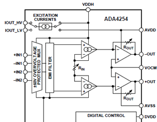
图1.ADA4254简化功能框图
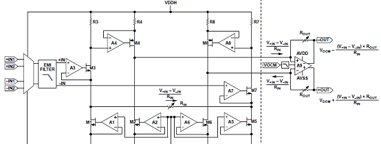
图2.ADA4254简化可编增益仪表放大器拓扑图

图3.ADA4254不支持SDO三态的SCS实现图
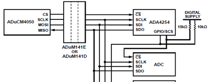
图4.所有器件支持SDO三态的SCS实现图
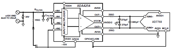
图5.ADA4254电压/电流输入应用电路图

图6.ADA4254三线RTD应用电路图
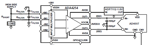
图7.ADA4254电流检测应用电路图
评估板ADA4254RU-EBZ
The ADA4254RU-EBZ evaluation board is designed to help users evaluate the ADA4254, which is offered in a 24-lead thin shrink small outline package (TSSOP) or a 28-lead lead framechip scale package (LFCSP). Figure 1 and Figure 2 show the front and back sides of the evaluation boards with the TSSOP package. The ADA4254RU-EBZ evaluation board is a 4-layer printedcircuit board (PCB).
The ADA4254RU-EBZ evaluation board requires the following three supply domains.A high voltage supply domain consisting of the supplypins, VDDH and VSSH, which are typically +28 V and −28 V respectively.
The analog output supply domain, AVDD, typically 5 V. The digital supply domain, DVDD, typically 3.3 V.
评估板ADA4254RU-EBZ主要特性:
Enables quick breadboarding and prototyping
Edge mounted SMA connector provisions
Easy connection to test equipment and other circuits

图8.评估板ADA4254RU-EBZ外形图(正面)
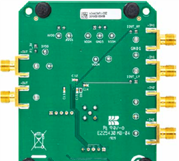
图9.评估板ADA4254RU-EBZ外形图(背面)
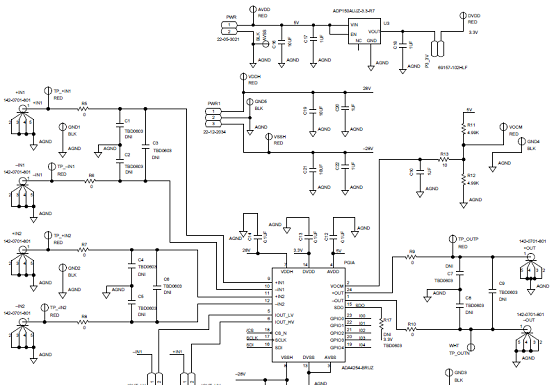
图10.评估板ADA4254RU-EBZ电路图(1)
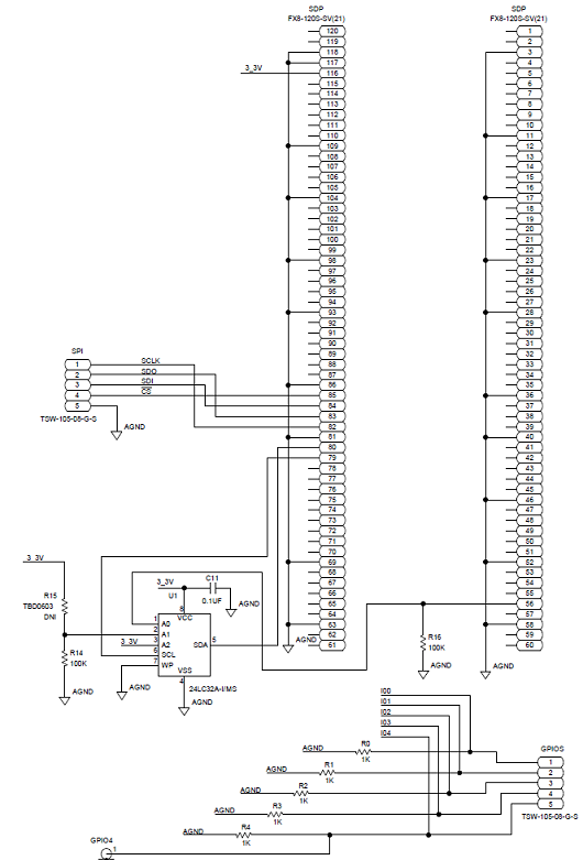
图11.评估板ADA4254RU-EBZ电路图(2)
评估板ADA4254RU-EBZ材料清单:

责任编辑:David
【免责声明】
1、本文内容、数据、图表等来源于网络引用或其他公开资料,版权归属原作者、原发表出处。若版权所有方对本文的引用持有异议,请联系拍明芯城(marketing@iczoom.com),本方将及时处理。
2、本文的引用仅供读者交流学习使用,不涉及商业目的。
3、本文内容仅代表作者观点,拍明芯城不对内容的准确性、可靠性或完整性提供明示或暗示的保证。读者阅读本文后做出的决定或行为,是基于自主意愿和独立判断做出的,请读者明确相关结果。
4、如需转载本方拥有版权的文章,请联系拍明芯城(marketing@iczoom.com)注明“转载原因”。未经允许私自转载拍明芯城将保留追究其法律责任的权利。
拍明芯城拥有对此声明的最终解释权。
相关资讯
:
基于MC33771主控芯片的新能源锂电池管理系统解决方案

AMIC110 32位Sitara ARM MCU开发方案

基于AMIC110多协议可编程工业通信处理器的32位Sitara ARM MCU开发方案

基于展讯SC9820超低成本LTE芯片平台的儿童智能手表解决方案

基于TI公司的AM437x双照相机参考设计

基于MTK6580芯片的W2智能手表解决方案


 2012- 2022 拍明芯城ICZOOM.com 版权所有 客服热线:400-693-8369 (9:00-18:00)


