


 产品分类
产品分类
Freescale MC9S08Lx超低功耗MCU开发方案
 90
90
 拍明
拍明
原标题:Freescale MC9S08Lx超低功耗MCU开发方案
freescale 公司的MC9S08Lx系列是集成了LCD驱动器的超低功耗MCU,同时增加了ADC的精度以用于医疗和仪表测控应用. MC9S08LH采用8位HCS08 CPU,有高达64KB的闪存,3.6V-2.1V电压时CPU频率高达40MHz,支持多达32个中断源,带电荷泵的多达8x36或4x40 LCD驱动器以及16位分辨率的ADC,主要应用在汽车电子,消费类电子,智能电表,工业控制,医疗和马达控制.本文介绍了MC9S08LH64系列主要特性,方框图以及TWR-S08LH64-KIT开发套件主要特性和开发板电路图.
Freescale expands the first S08 ultra-low-power MCU with LCD driver and increased ADC accuracy for medical and metering applications. The MC9S08LH family available with up to 64KB flash helps you reach your target performance levels while minimizing power consumption in your design, demonstrating extreme energy efficiency for ultra-long operation in battery-powered applications.
Maximize battery life, measure more precisely and make development easier with Freescale’s MC9S08LH64/36. The 16-bit SAR delivers outstanding precision to meet the needs of entry-level metering and medical applications.
Cost is reduced with the integration of an LCD driver which supports more segments with fewer pins. Additionally, the MCU is the industry’s best-in-class ultra-low-power MCU with LCD for long operation in batterypowered applications. These features are ideal for smart metering and medical applications such as glucometers and pulse oximeters.
Provides entry level flash-size part (64 KB) for cost-conscious, single-phase, electricity meter designs. The enhanced ADC, along with low-power technology, is ideal for electricity meters and medical devices operated by battery for more than five years.
MC9S08LH64系列主要特性:
Covers: MC9S08LH64 and MC9S08LH36
• 8-Bit HCS08 Central Processor Unit (CPU)
– Up to 40 MHz CPU at 3.6 V to 2.1 V across temperature range of –40℃ to 85℃
– Up to 20 MHz at 2.1 V to 1.8 V across temperature range of –40℃ to 85℃
HC08 instruction set with added BGND instruction
– Support for up to 32 interrupt/reset sources
• On-Chip Memory
– Dual array flash read/program/erase over full operating voltage and temperature
– Random-access memory (RAM)
– Security circuitry to prevent unauthorized access to RAM and flash contents
• Power-Saving Modes
– Two low-power stop modes
– Reduced-power wait mode
Low-power run and wait modes allow peripherals to run while voltage regulator is in standby
– Peripheral clock gating register can disable clocks to unused modules, thereby reducing currents
– Very low-power external oscillator that can be used in stop2 or stop3 modes to provide accurate clock source to time-of-day (TOD) module
– 6 μs typical wakeup time from stop3 mode
• Clock Source Options
– Oscillator (XOSC) — Loop-control Pierce oscillator; crystal or ceramic resonator range of 31.25 kHz to 38.4 kHz or 1 MHz to 16 MHz
– Internal Clock Source (ICS)—Internal clock source module containing a frequency-locked-loop (FLL) controlled by internal or external reference; precision trimming of internal reference allows 0.2% resolution and 2% deviation over temperature and voltage; supporting bus frequencies from 1 MHz to 20 MHz
• System Protection
– Watchdog computer operating properly (COP) reset with option to run from dedicated 1 kHz internal clock source or bus clock
– Low-voltage warning with interrupt
– Low-voltage detection with reset or interrupt
– Illegal opcode detection with reset; illegal address detection with reset
Flash block protection
• Development Support
– Single-wire background debug interface
– Breakpoint capability to allow single breakpoint setting during in-circuit debugging (plus two more breakpoints in on-chip debug module)
– On-chip in-circuit emulator (ICE) debug module containing three comparators and nine trigger modes
• Peripherals
– LCD — Up to 8×36 or 4×40 LCD driver with internal charge pump and option to provide an internally-regulated LCD reference that can be trimmed for contrast control
– ADC —16-bit resolution; with a dedicated differential ADC input, and 8 single-ended ADC inputs; up to 2.5 μs conversion time; hardware averaging; calibration registers, automatic compare function; temperature sensor; operation in stop3; fully functional from 3.6 V to 1.8 V
– IIC — Inter-integrated circuit bus module to operate at up to 100 kbps with maximum bus loading; multi-master operation; programmable slave address; interrupt-driven byte-by-byte data transfer; broadcast mode; 10-bit addressing
– ACMP — Analog comparator with selectable interrupt on rising, falling, or either edge of comparator output; compare option to fixed internal reference voltage; outputs can be
optionally routed to TPM module; operation in stop3
– SCIx — Two full-duplex non-return to zero (NRZ) modules (SCI1 and SCI2); LIN master extended break generation; LIN slave extended break detection; wakeup on active edge
– SPI — Full-duplex or single-wire bidirectional; double-buffered transmit and receive; master or slave mode; MSB-first or LSB-first shifting
– TPMx — Two 2-channel (TPM1 and TPM2); selectable input capture, output compare, or buffered edge- or center-aligned PWM on each channel
– TOD — (Time-of-day) 8-bit, quarter second counter with match register; external clock source for precise time base, time-of-day, calendar, or task scheduling functions
– VREFx—Trimmable via an 8-bit register in 0.5 mV steps; automatically loaded with room temperature value upon reset; can be enabled to operate in stop3 mode; trim register is not available in stop modes
• Input/Output
– Dedicated accurate voltage reference output pin, 1.2 V output (VREFOx); trimmable with 0.5 mV resolution
– Up to 39 GPIOs, two output-only pins
– Hysteresis and configurable pullup device on all input pins; configurable slew rate and drive strength on all output pins
• Package Options: 14mm × 14mm 80-pin LQFP, 10 mm × 10 mm 64-pin LQFP
MC9S08LH64系列目标应用:
Single phase electricity meters
Low-end utility metering
Portable medical equipments
Thermostats
Automated test equipments
Industrial process control and measurement
Sensor interfacing
Digital scales
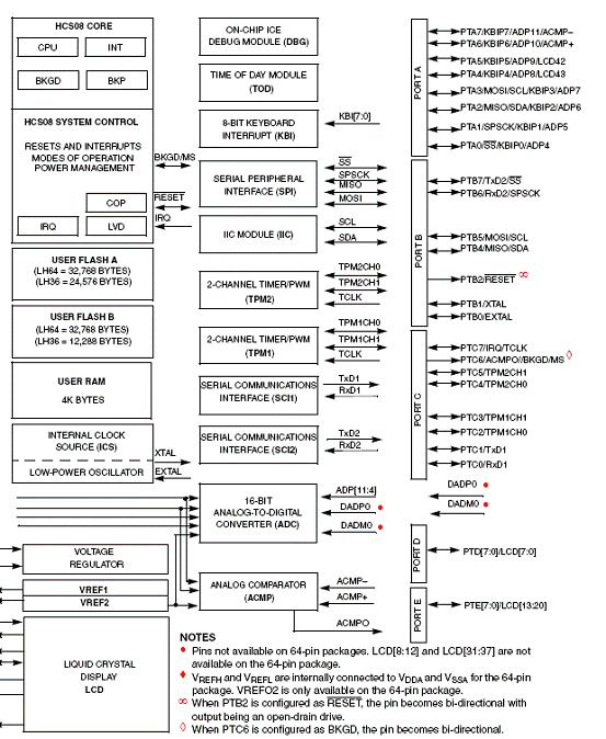
图1.MC9S08LH64系列方框图
TWR-S08LH64-KIT开发套件
The cost effective TWR-S08LH64-KIT development tool is part of the Tower System and features the MC9S08LH64 segment LCD controller with integrated 16 bit ADC. It provides everything designer needs to develop and evaluate application code. The integrated OSBDM allows a designer to comunicate with the board and target device with only a USB cable and the board highlights the MCU’s low power features.
This module is designed to be combined and used with a variety of peripheral modules in the Tower System, and can also operate as a standalone debug tool that can be purchased separately from the complete kit, part number TWR-S08LH64.
TWR-S08LH64-KIT开发套件主要特性:
5 K One Turn Potentiometer
RS232 port
MC9S08LH64 MCU
32,768 Hz Crystal
Freescale 3 axis accelerometer ADC input to MCU
Buzzer
Light Sensor with LP filter and opamp
Mini-B USB connector
1 reset push button and 4 push switches
2 x 28 segments LCD display
The TWR-S08LH64-KIT contains:
TWR-S08LH64 module - 8-bit Segment LCD module that features the MC9S08LH64
TWR-PROTO - Prototyping module with perfboard area
TWR-ELEV modules
Necessary cables
An interactive DVD with lab tutorials, software, training and collateral
A printed guide on how to quickly get started using the development kit
The TWR-S08LH64 module contains:
TWR-S08LH64 board
Necessary cables
An interactive DVD with lab tutorials, software, training and collateral
A printed guide on how to quickly get started

图2.TWR-S08LH64-KIT开发套件外形图
Specifications:
Board Size 3.55” x 3.20” overall
Power Input: +5V from USB connector or from Tower System
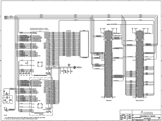
图3.TWR-S08LH64-KIT开发板电路图(1)
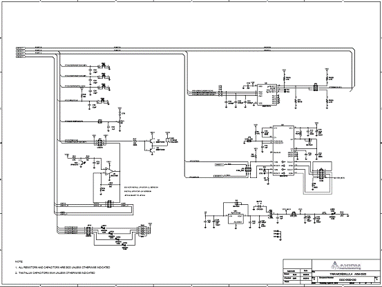
图4.TWR-S08LH64-KIT开发板电路图(2)
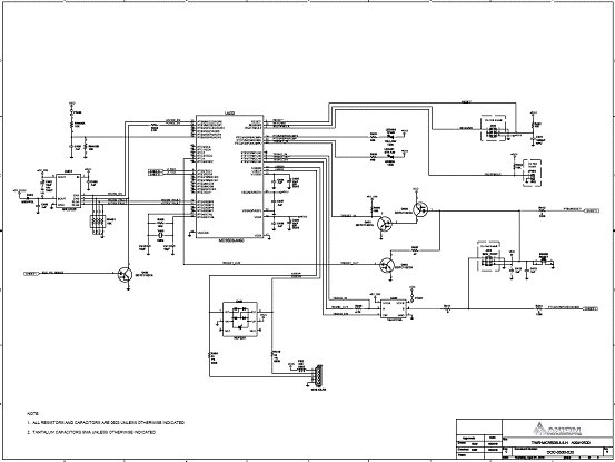
图5.TWR-S08LH64-KIT开发板电路图(3)
责任编辑:David
【免责声明】
1、本文内容、数据、图表等来源于网络引用或其他公开资料,版权归属原作者、原发表出处。若版权所有方对本文的引用持有异议,请联系拍明芯城(marketing@iczoom.com),本方将及时处理。
2、本文的引用仅供读者交流学习使用,不涉及商业目的。
3、本文内容仅代表作者观点,拍明芯城不对内容的准确性、可靠性或完整性提供明示或暗示的保证。读者阅读本文后做出的决定或行为,是基于自主意愿和独立判断做出的,请读者明确相关结果。
4、如需转载本方拥有版权的文章,请联系拍明芯城(marketing@iczoom.com)注明“转载原因”。未经允许私自转载拍明芯城将保留追究其法律责任的权利。
拍明芯城拥有对此声明的最终解释权。
相关资讯
:
基于MC33771主控芯片的新能源锂电池管理系统解决方案

AMIC110 32位Sitara ARM MCU开发方案

基于AMIC110多协议可编程工业通信处理器的32位Sitara ARM MCU开发方案

基于展讯SC9820超低成本LTE芯片平台的儿童智能手表解决方案

基于TI公司的AM437x双照相机参考设计

基于MTK6580芯片的W2智能手表解决方案


 2012- 2022 拍明芯城ICZOOM.com 版权所有 客服热线:400-693-8369 (9:00-18:00)


