


 产品分类
产品分类
EMBEST NXP LPC1768 ARM Cortex-M3 MCU开发方案
 84
84
 拍明
拍明
原标题:EMBEST NXP LPC1768 ARM Cortex-M3 MCU开发方案
NXP公司的LPC1768/66/65/64是基于ARM Cortex-M3的微控制器, 采用3级流水线和哈佛架构,具有单独的本地指令,数据总线和用于外设的第三条总线,其CPU工作频率高达100MHz,主要用于电表,照明,工业网络,告警系统,白色家电和马达控制.本文介绍了LPC1768/66/65/64主要特性,方框图, LPC1768评估板主要指标和详细电路图.
The LPC1768/66/65/64 are ARM Cortex-M3 based microcontrollers for embedded applications featuring a high level of integration and low power consumption. The ARM Cortex-M3 is a next generation core that offers system enhancements such as enhanced debug features and a higher level of support block integration.
The LPC1768/66/65/64 operates at CPU frequencies of up to 100 MHz. The ARM Cortex-M3 CPU incorporates a 3-stage pipeline and uses a Harvard architecture with separate local instruction and data buses as well as a third bus for peripherals. The ARM Cortex-M3 CPU also includes an internal prefetch unit that supports speculative branching.
The peripheral complement of the LPC1768/66/65/64 includes up to 512 kB of flash memory, up to 64 kB of data memory, Ethernet MAC, USB Device/Host/OTG interface, 8-channel general purpose DMA controller, 4 UARTs, 2 CAN channels, 2 SSP controllers, SPI interface, 3 I2C-bus interfaces, 2-input plus 2-output I2S-bus interface, 8-channel 12-bit ADC, 10-bit DAC, motor control PWM, Quadrature Encoder interface, 4 general purpose timers, 6-output general purpose PWM, ultra-low power Real-Time Clock (RTC) with separate battery supply, and up to 70 general purpose I/O pins.
The LPC1768/66/65/64 are pin-compatible to the 100-pin LPC236x ARM7-based microcontroller series.
LPC1768/66/65/64主要特性:
ARM Cortex-M3 processor, running at frequencies of up to 100 MHz. A Memory Protection Unit (MPU) supporting eight regions is included.
ARM Cortex-M3 built-in Nested Vectored Interrupt Controller (NVIC).
Up to 512 kB on-chip flash programming memory. Enhanced flash memory accelerator enables high-speed 100 MHz operation with zero wait states.
In-System Programming (ISP) and In-Application Programming (IAP) via on-chip bootloader software.
On-chip SRAM includes:
32/16 kB of SRAM on the CPU with local code/data bus for high-performance CPU access.
Two/one 16 kB SRAM blocks with separate access paths for higher throughput.These SRAM blocks may be used for Ethernet (LPC1768/66/64 only), USB, and DMA memory, as well as for general purpose CPU instruction and data storage.
Eight channel General Purpose DMA controller (GPDMA) on the AHB multilayer matrix that can be used with the SSP, I2S-bus, UART, the Analog-to-Digital and Digital-to-Analog converter peripherals, timer match signals, and for memory-to-memory transfers.
Multilayer AHB matrix interconnect provides a separate bus for each AHB master. AHB masters include the CPU, General Purpose DMA controller, Ethernet MAC (LPC1768/66/64 only), and the USB interface. This interconnect provides communication with no arbitration delays.
Split APB bus allows high throughput with few stalls between the CPU and DMA.
Serial interfaces:
Ethernet MAC with RMII interface and dedicated DMA controller (LPC1768/66/64 only).
USB 2.0 full-speed device/Host/OTG controller with dedicated DMA controller and on-chip PHY for device, Host, and OTG functions. The LPC1764 includes a device controller only.
Four UARTs with fractional baud rate generation, internal FIFO, DMA support, and RS-485 support. One UART has modem control I/O, and one UART has IrDA support.
CAN 2.0B controller with two channels.
SPI controller with synchronous, serial, full duplex communication and programmable data length.
Two SSP controllers with FIFO and multi-protocol capabilities. The SSP interfaces can be used with the GPDMA controller.
Two I2C-bus interfaces supporting fast mode with a data rate of 400 kbits/s with multiple address recognition and monitor mode.
One I2C-bus interface supporting full I2C-bus specification and fast mode plus with a data rate of 1 Mbit/s with multiple address recognition and monitor mode.
On the LPC1768/66/65 only, I2S (Inter-IC Sound) interface for digital audio input or output, with fractional rate control. The I2S-bus interface can be used with the GPDMA. The I2S-bus interface supports 3-wire and 4-wire data transmit and receive as well as master clock input/output.
Other peripherals:
70 General Purpose I/O (GPIO) pins with configurable pull-up/down resistors and a new, configurable open-drain operating mode.
12-bit Analog-to-Digital Converter (ADC) with input multiplexing among eight pins,conversion rates up to 1 MHz, and multiple result registers. The 12-bit ADC can be used with the GPDMA controller.
10-bit Digital-to-Analog Converter (DAC) with dedicated conversion timer and DMA support (LPC1768/66/65 only).
Four general purpose timers/counters, with a total of eight capture inputs and ten compare outputs. Each timer block has an external count input and DMA support.
One motor control PWM with support for three-phase motor control.
Quadrature encoder interface that can monitor one external quadrature encoder.
One standard PWM/timer block with external count input.
RTC with a separate power domain and dedicated RTC oscillator. The RTC block includes 64 bytes of battery-powered backup registers.
Watchdog Timer (WDT) resets the microcontroller within a reasonable amount of time if it enters an erroneous state.
System tick timer, including an external clock input option.
Repetitive interrupt timer provides programmable and repeating timed interrupts.
Each peripheral has its own clock divider for further power savings.
Standard JTAG test/debug interface for compatibility with existing tools. Serial Wire Debug and Serial Wire Trace Port options.
Emulation trace module enables non-intrusive, high-speed real-time tracing of instruction execution.
Integrated PMU (Power Management Unit) automatically adjusts internal regulators to minimize power consumption during Sleep, Deep sleep, Power-down, and Deep power-down modes.
Four reduced power modes: Sleep, Deep-sleep, Power-down, and Deep power-down.
Single 3.3 V power supply (2.4 V to 3.6 V).
Four external interrupt inputs configurable as edge/level sensitive. All pins on PORT0 and PORT2 can be used as edge sensitive interrupt sources.
Non-maskable Interrupt (NMI) input.
Clock output function that can reflect the main oscillator clock, IRC clock, RTC clock, CPU clock, and the USB clock.
The Wakeup Interrupt Controller (WIC) allows the CPU to automatically wake up from any priority interrupt that can occur while the clocks are stopped in deep sleep, Power-down, and Deep power-down modes.
Processor wake-up from Power-down mode via interrupts from various peripherals.
Brownout detect with separate threshold for interrupt and forced reset.
Power-On Reset (POR).
Crystal oscillator with an operating range of 1 MHz to 25 MHz.
4 MHz internal RC oscillator trimmed to 1 % accuracy that can optionally be used as a system clock.
PLL allows CPU operation up to the maximum CPU rate without the need for a high-frequency crystal. May be run from the main oscillator, the internal RC oscillator, or the RTC oscillator.
USB PLL for added flexibility.
Code Read Protection (CRP) with different security levels.
Available as 100-pin LQFP package (14 x14x1.4 mm).
LPC1768/66/65/64应用:
eMetering
Lighting
Industrial networking
Alarm systems
White goods
Motor control
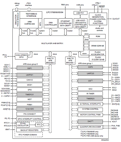
图1.LPC1768/66/65/64方框图
The LPC1768 evaluation board is based on ARM Cortex-M3 processor from NXP, its operating frequency is up to 100MHz, with 512KB high-speed on-Chip Flash Memory and 64KB RAM, together with a colour QVGA LCD, Ethernet, USB, CAN, SD/MMC card interface, and UARTs.
100MHz Cortex-M3, 512KB Flash,64KB SRAM
240x320 TFT LCD, 2.4"
Plenty of example source code
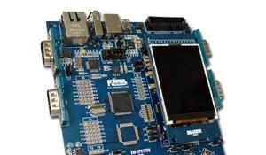
图2.LPC1768 ARM Cortex-M3 MCU开发板外形图
You can use the Cortex-M3 based LPC1768 Evaluation Board to generate and test application programs for the NXP LPC17xx microcontroller family. The LPC1768 Evaluation Board introduces the new NXP LPC1760 family of ARM Cortex-M3 processor-based devices, allowing you to create and test working programs for this advanced architecture, it has a wide range of interfaces making it a great starting point for your next Cortex-M3 project. With this hands-on process, you can determine the hardware and software requirements for current and future product development.
The LPC1768 Evaluation Board ships with the LPC1768 device that is a superset of several other device variants of the LPC17xx microcontroller series. The LPC1768 Board contains all the hardware components required in a single-chip LPC17xx system.
LPC1768评估板主要指标:
Hardware Specifications:
The connectors on the LPC1768 evaluation board provide easy access to many of the LPC1768’s on-chip peripherals.
USB 2.0 Full Speed Interface
Standard USB connectors for USB Device, USB-OTG, USB Host and UART via USB on the LPC1768 board for applications requiring USB communications.
Dual Serial Ports
Standard DB9 connectors are on the LPC1768 for both of the LPC1700’s serial ports. Your application may use either of these ports.
Dual CAN Ports
Standard DB9 connectors are on the LPC1768 board for applications requiring CAN communications. Your application may use either or both of these ports, or they may be disabled with a configuration jumper.
LCD Display
A detachable, 240x320 TFT, color LCD display. You may use this graphic display device to show real-time debug and program status messages.
MicroSD Card Connector
A MicroSD Card connector for developing applications requiring access to MicroSD Cards.
Joystick
A 5-position joystick. Your application may use this to control port pin input.
LF Amplifier
An LF Amplifier on the LPC1768 connects the D/A output of the LPC1700 device to a speaker. You may use this LF Amplifier to generate sound.
Analog Voltage Control for ADC Input
An adjustable analog voltage source is on the LPC1768 board for testing the Analog to Digital output feature of the LPC1700. A configuration jumper enables and disables this feature.
JTAG and Cortex/ETM Download and Debug
The LPC1768 board incorporates both a JTAG interface and a Cortex Debug + ETM interface. When coupled with the ULINK2 USB-JTAG adapter, the Serial Wire JTAG interface allows flash programming and debugging. With the ULINKPro adapter, the Cortex Debug/ETM interface allows flash programming and instruction trace debugging.
责任编辑:HanFeng
【免责声明】
1、本文内容、数据、图表等来源于网络引用或其他公开资料,版权归属原作者、原发表出处。若版权所有方对本文的引用持有异议,请联系拍明芯城(marketing@iczoom.com),本方将及时处理。
2、本文的引用仅供读者交流学习使用,不涉及商业目的。
3、本文内容仅代表作者观点,拍明芯城不对内容的准确性、可靠性或完整性提供明示或暗示的保证。读者阅读本文后做出的决定或行为,是基于自主意愿和独立判断做出的,请读者明确相关结果。
4、如需转载本方拥有版权的文章,请联系拍明芯城(marketing@iczoom.com)注明“转载原因”。未经允许私自转载拍明芯城将保留追究其法律责任的权利。
拍明芯城拥有对此声明的最终解释权。
相关资讯
:
基于MC33771主控芯片的新能源锂电池管理系统解决方案

AMIC110 32位Sitara ARM MCU开发方案

基于AMIC110多协议可编程工业通信处理器的32位Sitara ARM MCU开发方案

基于展讯SC9820超低成本LTE芯片平台的儿童智能手表解决方案

基于TI公司的AM437x双照相机参考设计

基于MTK6580芯片的W2智能手表解决方案


 2012- 2022 拍明芯城ICZOOM.com 版权所有 客服热线:400-693-8369 (9:00-18:00)


