


 产品分类
产品分类
Embest NXP LPC1788 32位ARM Cortex-M3 MCU开发方案
 143
143
 拍明
拍明
原标题:Embest NXP LPC1788 32位ARM Cortex-M3 MCU开发方案
Embest公司的EM-LPC1788开发板是基于NXP公司的LPC1788 32位ARM Cortex-M3 MCU,采用JTAG仿真和调试以及ISP编程,支持各种电源如USB2UART mini USB/USB1/USB2/EXT 5V,主要用在通信如POS终端,网络服务器和多协议桥,工业/医疗如自动化控制,应用控制,机器人控制,HVAC PLC和逆变器等,消费类电子如音频,MP3译码,告警系统,显示器,打印机和小型设备以及汽车电子如汽车告警,GPS监视器等.本文介绍了 LPC178x/7x系列主要特性和优势,框图,EM-LPC1788开发板硬件指标和软件指标,框图和电路图.
The LPC178x/7x is an ARM Cortex-M3 based microcontroller for embedded applications requiring a high level of integration and low power dissipation.
The Cortex-M3 is a next generation core that offers better performance than the ARM7 at the same clock rate and other system enhancements such as modernized debug features and a higher level of support block integration. The Cortex-M3 CPU incorporates a 3-stage pipeline and has a Harvard architecture with separate local instruction and data buses, as well as a third bus with slightly lower performance for peripherals. The Cortex-M3 CPU also includes an internal prefetch unit that supports speculative branches.
The LPC178x/7x adds a specialized flash memory accelerator to accomplish optimal performance when executing code from flash. The LPC178x/7x operates at up to 120 MHz CPU frequency.
The peripheral complement of the LPC178x/7x includes up to 512 kB of flash program memory, up to 96 kB of SRAM data memory, up to 4032 byte of EEPROM data memory, External Memory Controller (EMC), LCD (LPC178x only), Ethernet, USB Device/Host/OTG, a General Purpose DMA controller, five UARTs, three SSP controllers, three I2C-bus interfaces, one eight-channel, 12-bit ADC, a 10-bit DAC, a Quadrature Encoder Interface, four general purpose timers, two general purpose PWMs with six outputs each and one motor control PWM, an ultra-low power RTC with separate battery supply and event recorder, a windowed watchdog timer, a CRC calculation engine, up to 165 general purpose I/O pins, and more. The pinout of LPC178x/7x is intended to allow pin function compatibility with the LPC24xx and LPC23xx.
LPC178x/7x系列主要特性和优势:
Functional replacement for the LPC23xx and LPC24xx family devices.
System:
ARM Cortex-M3 processor, running at frequencies of up to 120 MHz. A Memory Protection Unit (MPU) supporting eight regions is included.
ARM Cortex-M3 built-in Nested Vectored Interrupt Controller (NVIC).
Multilayer AHB matrix interconnect provides a separate bus for each AHB master.
AHB masters include the CPU,USB, Ethernet, and the General Purpose DMA controller. This interconnect provides communication with no arbitration delays unless two masters attempt to access the same slave at the same time.
Split APB bus allows for higher throughput with fewer stalls between the CPU and DMA. A single level of write buffering allows the CPU to continue without waiting for completion of APB writes if the APB was not already busy.
Cortex-M3 system tick timer, including an external clock input option.
Standard JTAG test/debug interface as well as Serial Wire Debug and Serial WireTrace Port options.
Embedded Trace Macrocell (ETM) module supports real-time trace.
Boundary scan for simplified board testing.
Non-maskable Interrupt (NMI) input.
Memory:
Up to 512 kB on-chip flash program memory with In-System Programming (ISP)and In-Application Programming (IAP) capabilities. The combination of an enhanced flash memory accelerator and location of the flash memory on the CPU local code/data bus provides high code performance from flash.
Up to 96 kB on-chip SRAM includes:
64 kB of main SRAM on the CPU with local code/data bus for high-performance CPU access.
Two 16 kB peripheral SRAM blocks with separate access paths for higher throughput. These SRAM blocks may be used for DMA memory as well as for general purpose instruction and data storage.
Up to 4032 byte on-chip EEPROM.
LCD controller, supporting both Super-Twisted Nematic (STN) and Thin-Film Transistors (TFT) displays.
Dedicated DMA controller.
Selectable display resolution (up to 1024 x 768 pixels).
Supports up to 24-bit true-color mode.
External Memory Controller (EMC) provides support for asynchronous static memory devices such as RAM, ROM and flash, as well as dynamic memories such as single data rate SDRAM with an SDRAM clock of up to 80 MHz.
Eight channel General Purpose DMA controller (GPDMA) on the AHB multilayer matrix that can be used with the SSP, I2S, UART, CRC engine, Analog-to-Digital and Digital-to-Analog converter peripherals, timer match signals, GPIO, and for memory-to-memory transfers.
Serial interfaces:
Ethernet MAC with MII/RMII interface and associated DMA controller. These functions reside on an independent AHB.
USB 2.0 full-speed dual-port device/host/OTG controller with on-chip PHY and associated DMA controller.
Five UARTs with fractional baud rate generation, internal FIFO, DMA support, and RS-485/EIA-485 support. One UART (UART1) has full modem control I/O, and one UART (USART4) supports IrDA, synchronous mode, and a smart card mode conforming to ISO7816-3.
Three SSP controllers with FIFO and multi-protocol capabilities. The SSP controllers can be used with the GPDMA.
Three enhanced I2C-bus interfaces, one with a true open-drain output supporting the full I2C-bus specification and Fast-mode Plus with data rates of 1 Mbit/s, two with standard port pins. Enhancements include multiple address recognition and monitor mode.
I2S-bus (Inter-IC Sound) interface for digital audio input or output. It can be used with the GPDMA. CAN controller with two channels.
Digital peripherals:
SD/MMC memory card interface.
Up to 165 General Purpose I/O (GPIO) pins depending on the packaging with configurable pull-up/down resistors, open-drain mode, and repeater mode. All GPIOs are located on an AHB bus for fast access and support Cortex-M3 bit-banding. GPIOs can be accessed by the General Purpose DMA Controller. Any pin of ports 0 and 2 can be used to generate an interrupt.
Two external interrupt inputs configurable as edge/level sensitive. All pins on port 0 and port 2 can be used as edge sensitive interrupt sources.
Four general purpose timers/counters with a total of eight capture inputs and ten compare outputs. Each timer block has an external count input. Specific timer events can be selected to generate DMA requests.
Quadrature encoder interface that can monitor one external quadrature encoder.
Two standard PWM/timer blocks with external count input option.
One motor control PWM with support for three-phase motor control.
Real-Time Clock (RTC) with a separate power domain. The RTC is clocked by a dedicated RTC oscillator. The RTC block includes 20 bytes of battery-powered backup registers, allowing system status to be stored when the rest of the chip is powered off. Battery power can be supplied from a standard 3 V lithium button cell.
The RTC will continue working when the battery voltage drops to as low as 2.1 V. An RTC interrupt can wake up the CPU from any reduced power mode.
Event Recorder that can capture the clock value when an event occurs on any of three inputs. The event identification and the time it occurred are stored in registers. The Event Recorder is located in the RTC power domain and can therefore operate as long as there is RTC power.
Windowed Watchdog Timer (WWDT). Windowed operation, dedicated internal oscillator, watchdog warning interrupt, and safety features.
CRC Engine block can calculate a CRC on supplied data using one of three standard polynomials. The CRC engine can be used in conjunction with the DMA controller to generate a CRC without CPU involvement in the data transfer.
Analog peripherals:
12-bit Analog-to-Digital Converter (ADC) with input multiplexing among eight pins, conversion rates up to 400 kHz, and multiple result registers. The 12-bit ADC can be used with the GPDMA controller.
10-bit Digital-to-Analog Converter (DAC) with dedicated conversion timer and GPDMA support.
Power control:
Four reduced power modes: Sleep, Deep-sleep, Power-down, and Deep power-down.
The Wake-up Interrupt Controller (WIC) allows the CPU to automatically wake up from any priority interrupt that can occur while the clocks are stopped in Deep-sleep, Power-down, and Deep power-down modes.
Processor wake-up from Power-down mode via any interrupt able to operate during Power-down mode (includes external interrupts, RTC interrupt, PORT0/2 pin interrupt, and NMI).
Brownout detect with separate threshold for interrupt and forced reset.
On-chip Power-On Reset (POR).
Clock generation:
Clock output function that can reflect the main oscillator clock, IRC clock, RTC clock, CPU clock, USB clock, or the watchdog timer clock.
On-chip crystal oscillator with an operating range of 1 MHz to 25 MHz.
12 MHz Internal RC oscillator (IRC) trimmed to 1% accuracy that can optionally be used as a system clock.
An on-chip PLL allows CPU operation up to the maximum CPU rate without the need for a high-frequency crystal. May be run from the main oscillator or the internal RC oscillator.
A second, dedicated PLL may be used for USB interface in order to allow added flexibility for the Main PLL settings.
Versatile pin function selection feature allows many possibilities for using on-chip peripheral functions.
Unique device serial number for identification purposes.
Single 3.3 V power supply (2.4 V to 3.6 V). Temperature range of 40 C to 85 C.
Available as LQFP208, TFBGA208, TFBGA180, and LQFP144 package.
LPC178x/7x应用:
Communications:
Point-of-sale terminals, web servers, multi-protocol bridges
Industrial/Medical:
Automation controllers, application control, robotics control, HVAC, PLC, inverters, circuit breakers, medical scanning, security monitoring, motor drive, video intercom
Consumer/Appliance:
Audio, MP3 decoders, alarm systems, displays, printers, scanners, small appliances, fitness equipment
Automotive:
After-market, car alarms, GPS/fleet monitors
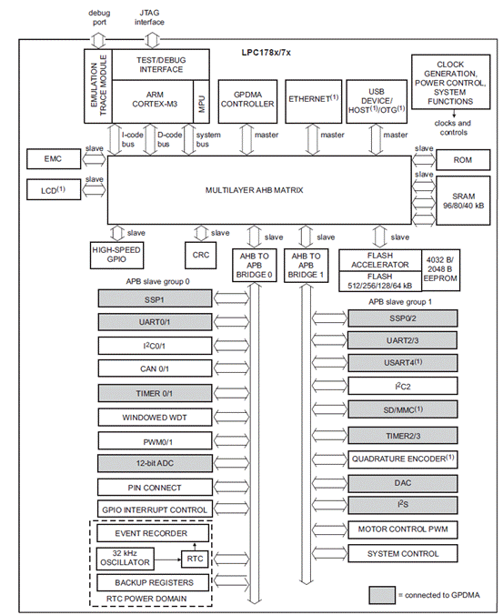
图1.LPC178x/7x方框图
EM-LPC1788开发板
EM-LPC1788 is a development board based on the main chip LPC1788 which is produced by NXP. The evaluation board is based on Cortex-M3 core, JTAG simulation and debug, and ISP programming. It supports variety of power supply, such as USB2UART mini USB/USB1/USB2/EXT 5V.
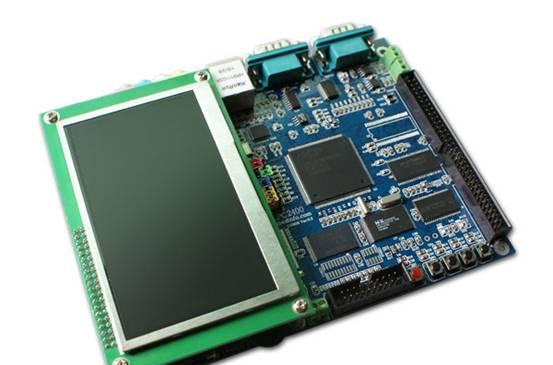
图2.EM-LPC1788开发板外形图
EM-LPC1788开发板硬件指标:
Hardware Specification: |
Hardware SpecificationDescriptionProcessorNXP LPC1788,Cortex-M3,120MHZMemoryInternal Memory:512KB SPI flash96KB SRAMExternal Memory:128MB NAND FLASH32MB SDRAM4MB NOR FLASH1MB SRAMDebug20-pin JTAG Debug interfaceSupport JTAG and SWD mode.StorageOne SD card interfaceSerialOne USB to Serial interfaceTwo UART interfaces and one of them can be used as modem interfaceUSBThree micro USB interfacesTwo USB Host interfacesCANTwo CAN interfacesAudioTwo I2S audio input interfacesTwo I2S audio output interfacesADCOne ADC adjustable potentiometerNetOne 10/100M Ethernet interfaceExpansion64-pin I/O user expansion interfaceKeysFour Push buttonOne Reset buttonPower SupplySupport USB2UART mini USB/USB1/USB2/EXT 5V |
EM-LPC1788开发板软件指标: |
ModuleExamplesRealize FunctionsADC01 ADC_InterruptADC Conversion in Interruption model02 ADC_PollingADC Conversion in Polling modelCAN03 Can_SelftestTest Can_Selftest modelCRC04 Crc_DemoApply in CRC via LPC1788DAC05 Dac_DmaSend or Receive data via DAC and DMA converter06 Dac_SineWaveGenerate sine wave via DACDMA07 DMA_Flash2RamTransmit data from flash to RAM to test GPDMAEEPROM08 EEprom_DemoEEPROM Work mechanism in LPC1788GPIO09 GPIO_InterruptTest GPIO Interruption function10 GPIO_LedBlinkyDrive LED to test GPIO Interruption functionNVIC11 Nvic_VectorTableRelocationVector Table RelocationEMC12 NandFlashTest Expansion Nandflash chip13 NorFlashTest Expansion Norflash chip14 SRAMTest Expansion SRAM chip15 SDRAMTest Expansion SDRAM chipPWM16 Pwm_SingleEdgeUse PWM signal in Single Edge model17 Pwm_DualEdgeGenerate PWM signal in Dual Edge model18 Pwm_MatchInterruptUse PWM match function in Interruption modelRTC19 Rtc_AlarmGenerate alarm interruption per 10 secondsSystick20 Systick_10msBaseConfigure system clock to generate interruption per 10 seconds.TIMER21 TIMER_MatchInterruptGenerate specific timePWR22 PWR_SleepMake system to Sleep mode and awaken by external interruption23 PWR_DeepSleepMake system to Deep sleep mode and awaken by external interruptionEMAC24 Emac_EasyWebEthernet port test,realize a simple web apply.LCD25 Lcd_LQ043T3DX0ATest LCD,Display specific picture26 Lcd_touchscreenTouchscreen testTouchScreen27 SSP_TouchscreenCatch Touchscreen coordinates via SSPWDT28 Wdt_InterruptGenerate interruption at a Specific time via WDT29 Wdt_ResetReset chip at a Specific time via WDTMCI30 Mci_CidCardTest SD card moduleUSB31 Usb_MassStorageBoard is mapped to be moving storage in PC32 Usb_VirtualComConfigure and make USB to be a virtual ComIIS33 IIS_AudioTest audio moduleIIC34_IIC_EEPROMRead and write external EEPROM via IICuC/OS35_UCOSII_V2.54Ucos Realtime system example test |
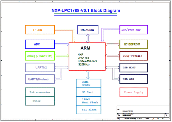
图3.EM-LPC1788开发板方框图

图4.EM-LPC1788开发板电路图(1)
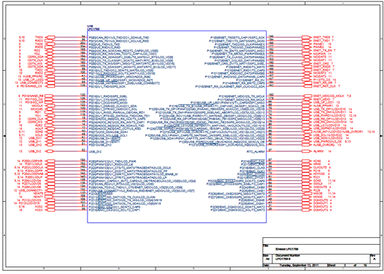
图5.EM-LPC1788开发板电路图(2)
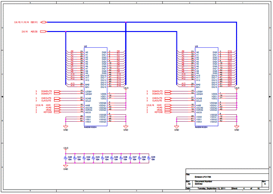
图6.EM-LPC1788开发板电路图(3)

图7.EM-LPC1788开发板电路图(4)
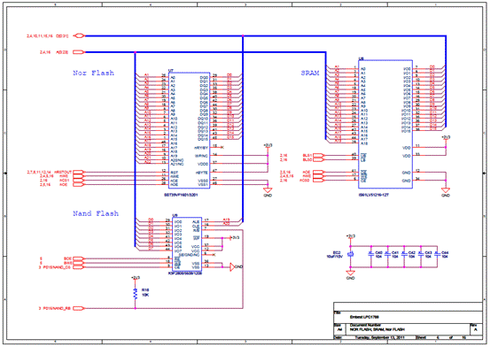
图8.EM-LPC1788开发板电路图(5)
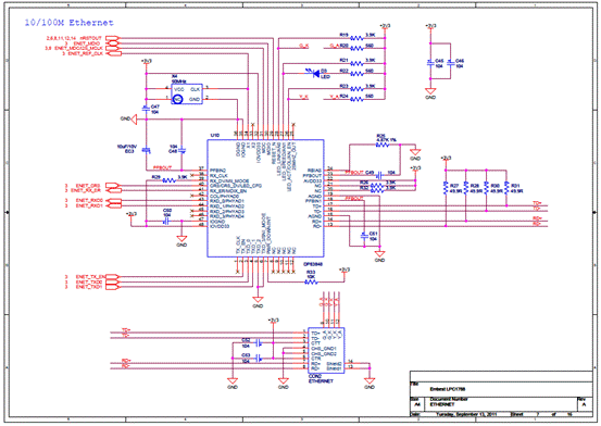
图9.EM-LPC1788开发板电路图(6)
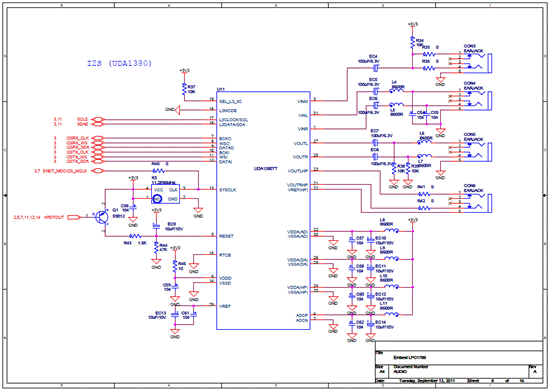
图10.EM-LPC1788开发板电路图(7)
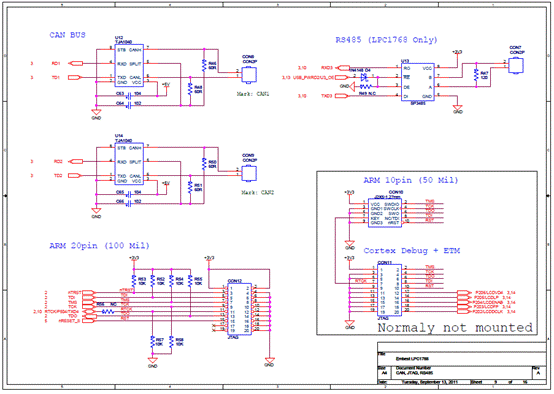
图11.EM-LPC1788开发板电路图(8)
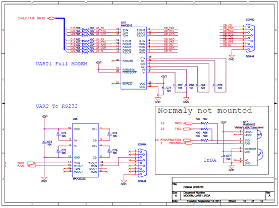
图12.EM-LPC1788开发板电路图(9)

图13.EM-LPC1788开发板电路图(10)

图14.EM-LPC1788开发板电路图(11)
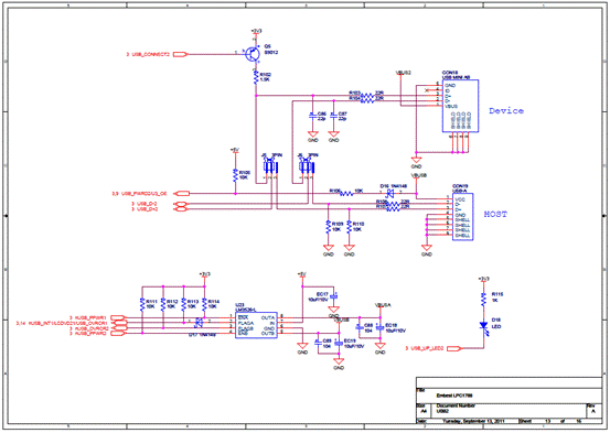
图15.EM-LPC1788开发板电路图(12)
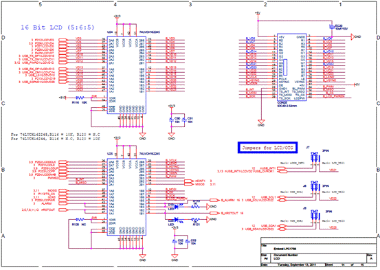
图16.EM-LPC1788开发板电路图(13)
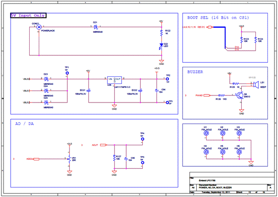
图17.EM-LPC1788开发板电路图(14)
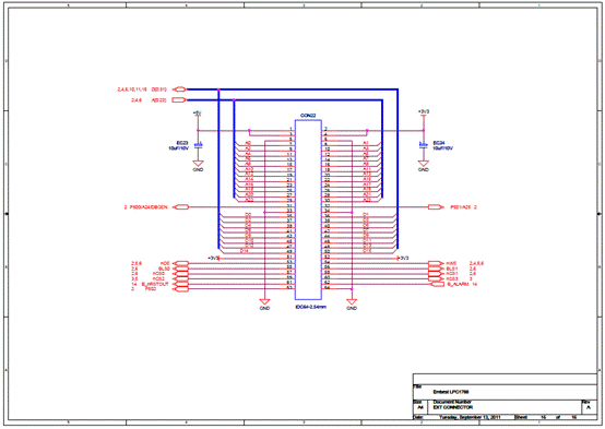
图18.EM-LPC1788开发板电路图(15)
责任编辑:HanFeng
【免责声明】
1、本文内容、数据、图表等来源于网络引用或其他公开资料,版权归属原作者、原发表出处。若版权所有方对本文的引用持有异议,请联系拍明芯城(marketing@iczoom.com),本方将及时处理。
2、本文的引用仅供读者交流学习使用,不涉及商业目的。
3、本文内容仅代表作者观点,拍明芯城不对内容的准确性、可靠性或完整性提供明示或暗示的保证。读者阅读本文后做出的决定或行为,是基于自主意愿和独立判断做出的,请读者明确相关结果。
4、如需转载本方拥有版权的文章,请联系拍明芯城(marketing@iczoom.com)注明“转载原因”。未经允许私自转载拍明芯城将保留追究其法律责任的权利。
拍明芯城拥有对此声明的最终解释权。
相关资讯
:
基于MC33771主控芯片的新能源锂电池管理系统解决方案

AMIC110 32位Sitara ARM MCU开发方案

基于AMIC110多协议可编程工业通信处理器的32位Sitara ARM MCU开发方案

基于展讯SC9820超低成本LTE芯片平台的儿童智能手表解决方案

基于TI公司的AM437x双照相机参考设计

基于MTK6580芯片的W2智能手表解决方案


 2012- 2022 拍明芯城ICZOOM.com 版权所有 客服热线:400-693-8369 (9:00-18:00)


