基于Microchip公司的MCP19117带MCU数字电源PWM控制方案
 287
287
 拍明
拍明
原标题:Microchip MCP19117带MCU数字电源PWM控制方案
microchip公司的MCP19117是具有改进性MCU的数字增强电源模拟同步低边PWM控制器,其标准的PIC MCU相当于PIC12F617,工作电压从4.5V到42V,适用于LED照明系统,电池充电器和其它低边PWM应用.本文介绍了MCP19117主要特性和MCU特性,功能框图和应用框图,以及可单独使用的MCP19117反激评估板主要特性,电路图,材料清单和PCB设计图.
The MCP19116/7 devices are highly integrated,mixed-signal low-side synchronous controllers thatoperate from +4.5V to +42V. The family features ananalog PWM controller with an integratedmicrocontroller core used for LED lighting systems,battery chargers and other low-side switch PWMapplications. The MCP19116/7 devices are derivedfrom the MCP19114/5 which share the same featuresand characteristics except for the addition of largerprogram memory (8k words vs 4k words) and severaldesign enhancements. These enhancements wereadded to the MCP19116/7 devices to improve
calibration, increase accuracy and provide greaterflexibility. The devices feature an analog internal PWMcontroller similar to the MCP1631, and a standard PIC®microcontroller similar to the PIC12F617.
Complete customization of device operatingparameters, start-up or shutdown profiles, protectionlevels and fault handling procedures are accomplishedby setting digital registers using Microchip’s MPLAB® XIntegrated Development Environment software and one of Microchip’s many in-circuit debugger and deviceprogrammers.
The MCP19116/7 mixed-signal low-side synchronouscontrollers feature integrated programmable inputUVLO/OVLO, programmable output overvoltage (OV),two low-side gate drive outputs with independentprogrammable dead time, programmable leading edgeblanking (four steps), programmable 6-bit slopecompensation and an integrated internalprogrammable oscillator for fixed-frequencyapplications.
An integrated 8-bit reference voltage (VREF)is used forsetting output current or voltage. An internalcomparator supports quasi-resonant applications.
Additional Capture and Compare modules areintegrated for increased control, including enhanceddimming capability.
The MCP19116/7 devices contain two internal LDOs. A5V LDO (VDD) is used to power the internal processorand provide 5V externally. A 4V LDO (AVDD) is used topower the internal analog circuitry. Either VDD or AVDDcan be connected internally to the 10-bit Analog-to-Digital Converter reference input. The 5Vexternal output can be used to supply the gate drive.
An analog filter between the VDD output and the VDRinput is recommended when implementing a 5V gatedrive supplied from VDD. Two 4.7 μF capacitors arerecommended with one placed as close as possible toVDD and one as close as possible to VDR, separated bya 10 isolation resistor. DO NOT exceed 10 μF on theVDD. An external supply is required to implementhigher gate drive voltages.
By utilizing a Microchip Technology IncorporatedTC1240A voltage doubler supplied from VDD to provideVDR, a 10V gate drive can be achieved.A 4V LDO is used to power the internal analog circuitry.
The two low-side drivers can be used to operate thepower converter in bidirectional mode, enabling the“shaping” of LED dimming current in LED applicationsor developing bidirectional power converters forbattery-powered applications.
The MCP19116 is packaged in a 24-lead 4 mm x 4 mmQFN. The MCP19117 is packaged in a 28-lead5 mm x 5 mm QFN.
The ability for system designers to configureapplication-specific features allows users of theMCP19116/7 devices to save costly board real estateand additional component costs.
The General Purpose Input/Output (GPIO) of theMCP19116/7 can be configured to offer a status output:
• a device enable, to control an external switch
• a switching frequency synchronization output orinput
• and even a device status or "heartbeat" indicatorWith integrated features like output current adjustmentand dynamic output voltage positioning,theMCP19116/7 family has the best in-class performanceand highest integration level currently available.
Power trains supported by this architecture include butare not limited to boost, flyback, quasi-resonantflyback, SEPIC, Ćuk, etc.
Two low-side gate drivers are capable of sinking andsourcing 1A at 10V VDR. With a 5V gate drive, thedriver is capable of 0.5A sink and source. The user hasthe option to allow the VIN UVLO to shut down thedrivers by setting the UVLOEN bit. When this bit is notset, the device drivers will ride through the UVLOcondition and continue to operate until VDR reaches thegate drive UVLO value. This value is selectable at 2.7Vor 5.4V and is always enabled. An internal reset for themicrocontroller core is set to 2.0V. An internalcomparator module is used to sense the desaturationof the flyback transformer to synchronize switching forquasi-resonant applications.
The operating input voltage for normal device operationranges from +4.5V to +42V with an absolute maximumof 44V. The maximum transient voltage is 48V for500 ms. An I2C serial bus is used for devicecommunications from the PWM controller to thesystem.
MCP19117主要特性:
• Input Voltage: +4.5V to +42V
• Can be configured with multiple topologies includingbut not limited to:
- Flyback
- Ćuk
- Boost
- SEPIC (Single-Ended Primary-InductorConverter)
• Capable of Quasi-Resonant or Fixed-FrequencyOperation
• Low Quiescent Current: 5 mA Typical
• Low Sleep Current: 50 μA Typical
• Low-Side Gate Drivers:
- +5V gate drive with 0.5A sink/source current
- +10V gate drive with 1A sink/source current
• Peak Current Mode Control
• Differential Remote Output Sense
• Multiple Output Systems:
- Master or Slave
• AEC-Q100 Qualified
• Configurable Parameters:
- VREF, Precision IOUT/VOUT Set Point (DAC)
- ADC Reference Switch (VDD or AVDD)
- Input Undervoltage Lockout (UVLO)
- Input Overvoltage Lockout (OVLO)
- Detection and protection
- Primary current leading edge blanking (0 ns,50 ns, 100 ns and 200 ns)
- Gate drive dead time (16 ns to 256 ns)
- Fixed switching frequency range:31.25 kHz to 2.0 MHz
- Slope compensation
- Quasi-Resonant configuration with built-incomparator and programmable offset voltage adjustment
- Primary current offset adjustment
- GPIO pin options
• Integrated Low-Side Differential Current-SenseAmplifier
• Better than 5% Current Regulation
• Thermal Shutdown
MCP19117 MCU特性:
• Precision 8 MHz Internal Oscillator Block:
- Factory-calibrated to ±1%, typical
• Interrupt-Capable:
- Firmware
- Interrupt-on-change pins
• Only 35 Instructions to Learn
• 8192 Words On-Chip Program Memory
• High-Endurance Flash:
- 100,000 write Flash endurance
- Flash retention: > 40 years
• Watchdog Timer (WDT) with IndependentOscillator for Reliable Operation
• Programmable Code Protection
• In-Circuit Serial Programming™ (ICSP™) via TwoPins
• Eight I/O Pins and One Input-Only Pin:
- Two open-drain pins
• Analog-to-Digital Converter (ADC):
- 10-bit resolution
- Five external channels
• Timer0: 8-bit Timer/Counter with 8-bit Prescaler
• Enhanced Timer1:
- 16-bit timer with prescaler
- Two selectable clock sources
• Timer2: 8-Bit Timer with Prescaler:
- 8-bit period register
• I2C Communication:
- 7-bit address masking
- Two dedicated address registers
• Addressable Universal Synchronous ReceiverTransmitter (AUSART) Modes
- Asynchronous (Full Duplex)
- Synchronous - Master (Half Duplex)
- Synchronous - Slave (Half Duplex)

图1.MCP19117反激同步准谐振框图

图2.MCP19117 CUK同步正输出应用框图

图3.MCP19116升压倒多准谐振应用框图

图4.MCP19117 MCU内核框图
MCP19117反激评估板
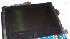
The MCP19117-Flyback Standalone Evaluation Board and Graphical User Interface (GUI) demonstrate the MCP19117 performance in a synchronous Flyback topology. It is configured to regulate load current, and is well suited to drive LED loads. Nearly all operational and control system parameters are programmable through the integrated PIC MCU core. The MCP19117 evaluation board comes preprogrammed with firmware designed to operate with the GUI interface. Microchip’s MPLABX IDE (Integrated Development Environment) can be used to develop and program user-defined firmware, thus customizing it to the specific application. The evaluation board contains headers for ICSP™ (In-Circuit Serial Programming), I2C™ communication as well as UART Full/Half Duplex modes. Several test points have been designed into the PWB for easy access and development purposes. The MCP19117-Flyback Standalone Evaluation Board also demonstrates an optimized PCB (Printed Circuit Board) layout that minimizes parasitic inductance, while increasing efficiency and power density. Proper PCB layout is critical to achieve optimum MCP19117 operation as well as power train efficiency and noise minimization.

图5.MCP19117反激评估板外形图
MCP19117反激评估板主要特性:
8K words Program Memory, 336 bytes RAM Memory
Vin range: 8V to 24V
Adjustable Iout current range: 1mA to 500mA
Vout range: 0V to 50V
Programming and I2C communication headers
UART Communication
The factory programmed source code is available
MCP19117反激评估板材料清单:


MCP19117反激评估板机械材料清单:

责任编辑:HanFeng
【免责声明】
1、本文内容、数据、图表等来源于网络引用或其他公开资料,版权归属原作者、原发表出处。若版权所有方对本文的引用持有异议,请联系拍明芯城(marketing@iczoom.com),本方将及时处理。
2、本文的引用仅供读者交流学习使用,不涉及商业目的。
3、本文内容仅代表作者观点,拍明芯城不对内容的准确性、可靠性或完整性提供明示或暗示的保证。读者阅读本文后做出的决定或行为,是基于自主意愿和独立判断做出的,请读者明确相关结果。
4、如需转载本方拥有版权的文章,请联系拍明芯城(marketing@iczoom.com)注明“转载原因”。未经允许私自转载拍明芯城将保留追究其法律责任的权利。
拍明芯城拥有对此声明的最终解释权。


 产品分类
产品分类




 2012- 2022 拍明芯城ICZOOM.com 版权所有 客服热线:400-693-8369 (9:00-18:00)


