Microchip PIC16(L)F18446 8位MCU的XLP MCU开发方案
 973
973
 拍明
拍明
microchip公司的PIC16(L)F18446是8位MCU,具有高分辨率智能模拟和核独立外设(CIP),集成了具有计算的12位ADC(ADC2),多种通信接口,温度传感器和存储器特性如内存访问分区(MAP)和器件信息区域(DIA),MCU具有多达28KB闪存和2KB RAM.这种超低功耗(XLP)MCU广泛用在通用领域和低功耗应用.本文介绍了PIC16(L)F18446主要特性,框图,以及MPLAB® Xpress PIC16F18446评估板主要特性,电路图,材料清单和PCB设计图.
PIC16(L)F184XX microcontrollers feature Intelligent Analog, Core Independent Peripherals (CIPs) andcommunication peripherals combined with eXtreme Low-Power (XLP) for a wide range of generalpurpose and low-power applications. Features such as a 12-bit Analog-to-Digital Converter withComputation (ADC2), Memory Access Partitioning (MAP), the Device Information Area (DIA), Powersavingoperating modes, and Peripheral Pin Select (PPS), offer flexible solutions for a wide variety ofcustom applications.
PIC16(L)F18446主要特性:
内核
• C Compiler Optimized RISC Architecture
• Only 50 Instructions
• Operating Speed:
– DC – 32 MHz clock input
– 125 ns minimum instruction cycle
• Interrupt Capability
• 16-Level Deep Hardware Stack
• Timers:
– Up to two 24-bit timers
– Up to four 8-bit timers
– Up to four 16-bit timers
• Low-Current Power-on Reset (POR)
• Configurable Power-up Timer (PWRT)
• Brown-out Reset (BOR)
• Low-Power BOR (LPBOR) Option
• Windowed Watchdog Timer (WWDT):
– Variable prescaler selection
– Variable window size selection
– Configurable in hardware (Configuration Words) and/or software
• Programmable Code Protection
存储器
• Up to 28 KB Program Flash Memory
• Up to 2 KB Data SRAM Memory
• 256B Data EEPROM
• Direct, Indirect and Relative Addressing modes
• Memory Access Partition (MAP):
– Write-protect
– Customizable partition
• Device Information Area (DIA)
• Device Configuration Information (DCI)
工作特性
• Operating Voltage Range:
– 1.8V to 3.6V (PIC16LF184XX)
– 2.3V to 5.5V (PIC16F184XX)
• Temperature Range:
– Industrial: -40℃ to 85℃
– Extended: -40℃ to 125℃
省电工作模式
• Doze: CPU and Peripherals Running at Different Cycle Rates (typically CPU is lower)
• Idle: CPU Halted While Peripherals Operate
• Sleep: Lowest Power Consumption
• Peripheral Module Disable (PMD):
– Ability to selectively disable hardware module to minimize active power consumption of unused
peripherals
• Extreme Low-Power mode (XLP)
– Sleep: 500 nA typical @ 1.8V
– Sleep and Watchdog Timer: 900 nA typical @ 1.8V
eXtreme低功耗 (XLP)特性
• Sleep mode: 50 nA @ 1.8, typical
• Watchdog Timer: 500 nA @ 1.8V, typical
• Secondary Oscillator: 500 nA @ 32 kHz
• Operating Current:
– 8 uA @ 32 kHz, 1.8V, typical
– 32 uA/MHz @ 1.8V, typical
数字外设
• Configurable Logic Cell (CLC):
– 4 CLCs
– Integrated combinational and sequential logic
• Complementary Waveform Generator (CWG):
– 2 CWGs
– Rising and falling edge dead-band control
– Full-bridge, half-bridge, 1-channel drive
– Multiple signal sources
• Capture/Compare/PWM (CCP) modules:
– 4 CCPs
– 16-bit resolution for Capture/Compare modes
– 10-bit resolution for PWM mode
• Pulse-Width Modulators (PWM):
– 2 10-bit PWMs
• Numerically Controlled Oscillator (NCO):
– Precision linear frequency generator (@50% duty cycle) with 0.0001% step size of source inputclock
– Input Clock: 0 Hz – Resolution: fNCO/220
• Peripheral Pin Select (PPS):
– I/O pin remapping of digital peripherals
• Serial Communications:
– EUSART
• 1 EUSART(s)
• RS-232, RS-485, LIN compatible
• Auto-Baud Detect, Auto-wake-up on Start.
– Master Synchronous Serial Port (MSSP)
• 2 MSSP(s)
• SPI
• I2C, SMBus and PMBus™ compatible
• Data Signal Modulator (DSM)
– Modulates a carrier signal with digital data to create custom carrier synchronized output
waveforms
• Up to 18 I/O Pins:
– Individually programmable pull-ups
– Slew rate control
– Interrupt-on-change with edge-select
– Input level selection control (ST or TTL)
– Digital open-drain enable
• Timer modules:
– Timer0:
• 8/16-bit timer/counter
• Synchronous or asynchronous operation
• Programmable prescaler/postscaler
• Time base for capture/compare function
– Timer1/3/5 with gate control:
• 16-bit timer/counter
• Programmable internal or external clock sources
• Multiple gate sources
• Multiple gate modes
• Time base for capture/compare function
– Timer2/4/6 with Hardware Limit Timer:
• 8-bit timers
• Programmable prescaler/postscaler
• Time base for PWM function
• Hardware Limit (HLT) and one-shot extensions
• Selectable clock sources
– Signal Measurement Timer (SMT)
• 1 SMT(s)
• 24-bit timer/counter with programmable prescaler
模拟外设
• Analog-to-Digital Converter with Computation (ADC2):
– 12-bit with up to 17 external channels
– Conversion available during Sleep
– Automated post-processing
– Automated math functions on input signals:
• Averaging, filter calculations, oversampling and threshold comparison
– Integrated charge pump for low-voltage operation
– CVD support
• Zero-Cross Detect (ZCD):
– AC high voltage zero-crossing detection for simplifying TRIAC control
– Synchronized switching control and timing
• Temperature Sensor Circuit
• Comparator:
– 2 Comparators
– Fixed Voltage Reference at (non)inverting input(s)
– Comparator outputs externally accessible
• Digital-to-Analog Converter (DAC):
– 5-bit resolution, rail-to-rail
– Positive Reference Selection
– Unbuffered I/O pin output
– Internal connections to ADCs and comparators
• Fixed Voltage Reference (FVR) module:
– 1.024V, 2.048V and 4.096V output levels
灵活振荡器架构
• High-Precision Internal Oscillator:
– Software-selectable frequency range up to 32 MHz
– ±2% at calibration (nominal)
• 4x PLL for use with external sources
– up to 32 MHz (4-8 MHz input)
• 2x PLL for use with the HFINTOSC
– up to 32 MHz
• Low-Power Internal 31 kHz Oscillator (LFINTOSC)
• External 32.768 kHz Crystal Oscillator (SOCS)
• External Oscillator Block with:
– Three crystal/resonator modes up to 20 MHz
– Three external clock modes up to 32 MHz
– Fail-Safe Clock Monitor
• Detects clock source failure
– Oscillator Start-up Timer (OST)
• Ensures stability of crystal oscillator sources
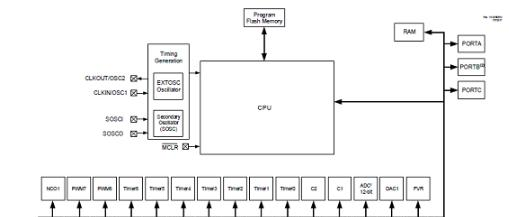
图1.PIC16(L)F18426/46框图
MPLAB® Xpress PIC16F18446评估板
Brilliant ideas are fleeting. As soon as they are recognized, they must be captured quickly, and made real with the highest possible urgency. In embedded design, the creative process is often blunted by the massive array of choices required to simply begin the development cycle. The tasks of selecting a target MCU, finding the appropriate tool chain, and setting everything up on your PC can keep your best ideas from becoming great products. The MPLAB Xpress PIC16F18446 Evaluation Board was designed with a single objective – to help your ideas take the shortest journey from imagination to reality.
MPLAB® Xpress PIC16F18446评估板主要特性:
Compact footprint offers flexibility during prototyping phase
On-board 8-bit MCUs support a wide range of applications
Integrated drag-and-drop Programmer with USB Interface
Integrates seamlessly with MPLAB Xpress IDE and MPLAB Code Configurator for the quickest development
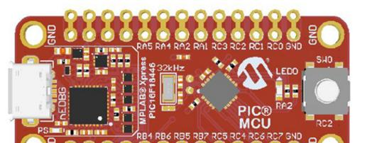
图2.MPLAB® Xpress PIC16F18446评估板外形图
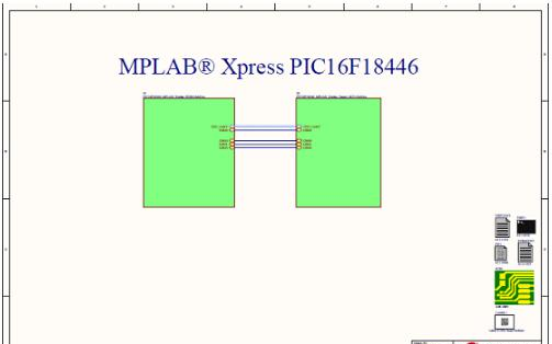
图3.MPLAB® Xpress PIC16F18446评估板电路图(1)
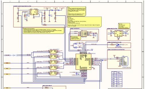
图4.MPLAB® Xpress PIC16F18446评估板电路图(2)
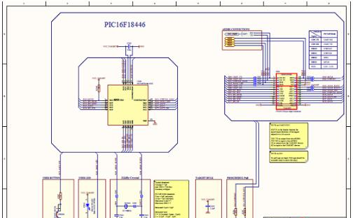
图5.MPLAB® Xpress PIC16F18446评估板电路图(3)
MPLAB® Xpress PIC16F18446评估板材料清单:
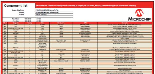
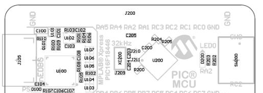
图6.MPLAB® Xpress PIC16F18446评估板PCB设计图(1)
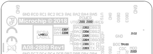
图7.MPLAB® Xpress PIC16F18446评估板PCB设计图(2)
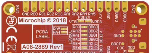
图8.MPLAB® Xpress PIC16F18446评估板PCB设计图(3)
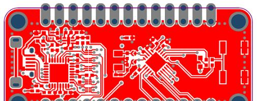
图9.MPLAB® Xpress PIC16F18446评估板PCB设计图(4)
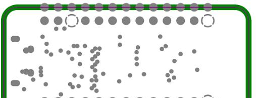
图10.MPLAB® Xpress PIC16F18446评估板PCB设计图(5)
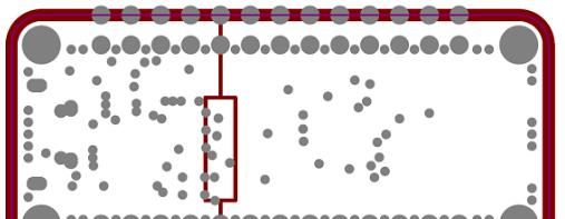
图11.MPLAB® Xpress PIC16F18446评估板PCB设计图(6)
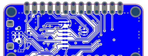
图12.MPLAB® Xpress PIC16F18446评估板PCB设计图(7)
责任编辑:Davia
【免责声明】
1、本文内容、数据、图表等来源于网络引用或其他公开资料,版权归属原作者、原发表出处。若版权所有方对本文的引用持有异议,请联系拍明芯城(marketing@iczoom.com),本方将及时处理。
2、本文的引用仅供读者交流学习使用,不涉及商业目的。
3、本文内容仅代表作者观点,拍明芯城不对内容的准确性、可靠性或完整性提供明示或暗示的保证。读者阅读本文后做出的决定或行为,是基于自主意愿和独立判断做出的,请读者明确相关结果。
4、如需转载本方拥有版权的文章,请联系拍明芯城(marketing@iczoom.com)注明“转载原因”。未经允许私自转载拍明芯城将保留追究其法律责任的权利。
拍明芯城拥有对此声明的最终解释权。


 产品分类
产品分类




 2012- 2022 拍明芯城ICZOOM.com 版权所有 客服热线:400-693-8369 (9:00-18:00)


