


 产品分类
产品分类
基于Linear公司的LTC3897PolyPhase同步升压转换器解决方案
 261
261
 拍明
拍明
原标题:Linear LTC3897PolyPhase同步升压转换器解决方案
Linear公司的LTC3897是带输入/输出保护的PolyPhase™同步升压转换器,能驱动两个N沟功率MOSFET级,输入电压4.5V-65V(高达75V浪涌),输出高达65V,主要用在工业,汽车和军事/航空航天.本文介绍了LTC3897主要特性,框图和十多种应用电路,以及演示板DC2108主要特性,电路图和材料清单.
The LTC.3897 is a synchronous boost DC/DC controller with surge stopper and ideal diode controller. The boost controller drives two N-channel power MOSFET stages out-of-phase to reduce input and output capacitor requirements, allowing the use of smaller inductors than the single-phase equivalent. Synchronous rectification reduces power loss and eases thermal requirements.
The surge stopper controls the gate of an external N-channel MOSFET to protect against high voltage input transients and provides in-rush current control, overcurrent protection and output disconnect for the boost converter. The integrated ideal diode controller drives another N-channel MOSFET to replace a Schottky diode for reverse input protection and
voltage holdup or peak detection. It controls the forward voltage drop across the MOSFET and minimizes reverse current flow.
The LTC3897 is available in thermally-enhanced 38-pin leadless QFN or 38-lead TSSOP packages.
LTC3897主要特性:
nn Input Supply Range: 4.5V to 65V (Up to 75V Surge)
nn Reverse Input Protection to –40V
nn In-Rush Current Control, Overcurrent Protection and Output Disconnect for Boost Converter
nn Input Voltage Surge Protection with Adjustable Clamp Voltage
nn Onboard Ideal Diode Controller
nn Low Quiescent Current: 55μA
nn 2-Phase Operation Reduces Required Input and Output Capacitance and Noise
nn Output Voltage Up to 60V
nn Adjustable Gate Drive Level 5V to 10V (OPTI-DRIVE) for Logic-Level or Standard Threshold FETs
nn No External Bootstrap Diodes Required
LTC3897应用:
nn Industrial
nn Automotive
nn Military/Avionics

图1. LTC3897框图

图2. LTC3897应用电路图(1):24V/10A 2相同步升压转换器

图3. LTC3897应用电路图(2):3相工作

图4. LTC3897应用电路图(3):4相工作

图5. LTC3897应用电路图(4):6相工作
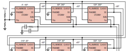
图6. LTC3897应用电路图(5):12相工作

图7. LTC3897应用电路图(6):高效2相48V升压转换器(1)

图8. LTC3897应用电路图(7):高效2相48V升压转换器(2)

图9. LTC3897应用电路图(8):高效2相24V升压转换器

图10. LTC3897应用电路图(9):高效2相48V升压转换器(3)

图11. LTC3897应用电路图(10):高效2相48V升压转换器(4)

图12. LTC3897应用电路图(11):高效2相48V升压转换器(5)

图13. LTC3897应用电路图(12):非同步107V/1.5A 2相48V升压转换器
演示板DC2108
Demonstration circuit DC2108 is DC/DC boost converter featuring the LTCR3897 constant frequency current mode boost controller. The DC2108A operates over a 16V to
55V input and provides 4A to 12A of output current. The 160kHz (2 •160kHz at the output) constant frequency operation results in a small and efficient circuit. The converter provides high output voltage accuracy (typically ±3%) over a wide load range with no minimum load requirement. The demonstration circuit can be easily modified to generate different output voltages.
The DC2108 has small circuit footprint. It is a high performance and cost effective solution for Telecom, Automotive and Power Over Ethernet applications.
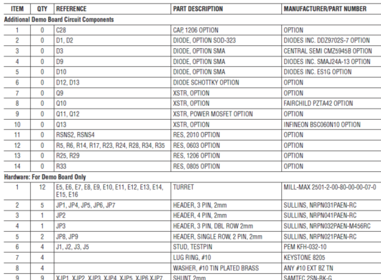
演示板DC2108材料清单:

责任编辑:HanFeng
【免责声明】
1、本文内容、数据、图表等来源于网络引用或其他公开资料,版权归属原作者、原发表出处。若版权所有方对本文的引用持有异议,请联系拍明芯城(marketing@iczoom.com),本方将及时处理。
2、本文的引用仅供读者交流学习使用,不涉及商业目的。
3、本文内容仅代表作者观点,拍明芯城不对内容的准确性、可靠性或完整性提供明示或暗示的保证。读者阅读本文后做出的决定或行为,是基于自主意愿和独立判断做出的,请读者明确相关结果。
4、如需转载本方拥有版权的文章,请联系拍明芯城(marketing@iczoom.com)注明“转载原因”。未经允许私自转载拍明芯城将保留追究其法律责任的权利。
拍明芯城拥有对此声明的最终解释权。
相关资讯
:
基于MC33771主控芯片的新能源锂电池管理系统解决方案

AMIC110 32位Sitara ARM MCU开发方案

基于AMIC110多协议可编程工业通信处理器的32位Sitara ARM MCU开发方案

基于展讯SC9820超低成本LTE芯片平台的儿童智能手表解决方案

基于TI公司的AM437x双照相机参考设计

基于MTK6580芯片的W2智能手表解决方案


 2012- 2022 拍明芯城ICZOOM.com 版权所有 客服热线:400-693-8369 (9:00-18:00)


