


 产品分类
产品分类
TI F2837xD单相逆变器参考设计TIDM-HV-1PH-DCAC
 203
203
 拍明
拍明
原标题:TI F2837xD单相逆变器参考设计TIDM-HV-1PH-DCAC
TI公司的tms320F2837xD是功能强大的32位浮点微控制器(MCU),支持新双核C28x架构,大大提升了系统性能,每核信号处理性能200MHz,集成模拟和控制外设使高端系统的设计者合并控制体系结构,不需要多个处理器;器件还集成了512KB (256KW)或1MB (512KW)闪存(ECC保护), 172KB (86KW)或204KB (102KW) RAM(ECC保护或奇偶校验位保护),支持第三方开发的双区安全以及唯一识别号码.满足汽车应用的AEC Q100规范,主要用在先进驾驶辅助系统(ADAS),建筑物自动化,POS终端,EV/HEV动力传动,工厂自动化,电网架构,工业传输,医疗,健康和健美设备,马达驱动,供电,通信设备,测试和测量.本文介绍了TMS320F2837x9主要特性,框图,采用C2000™ F2837xD MCU单相逆变器(DC/AC)参考设计TIDM-HV-1PH-DCAC主要特性和性能指标,电路图和材料清单.
The Delfino™ TMS320F2837xD is a powerful 32-bit floating-point microcontroller unit (MCU) designed for advanced closed-loop control applications such as industrial drives and servo motor control; solar inverters and converters; digital power; transportation; and power line communications. Complete development packages for digital power and industrial drives are available as part of the powerSUITE and DesignDRIVE initiatives. While the Delfino product line is not new to the TMS320C2000™ portfolio, the F2837xD supports a new dual-core C28x architecture that significantly boosts system performance. The integrated analog and control peripherals also let designers consolidate control architectures and eliminate multiprocessor use in high-end systems.
The dual real-time control subsystems are based on TI’s 32-bit C28x floating-point CPUs, which provide 200 MHz of signal processing performance in each core. The C28x CPUs are further boosted by the new TMU accelerator, which enables fast execution of algorithms with trigonometric operations common in transforms and torque loop calculations; and the VCU accelerator, which reduces the time for complex math operations common in encoded applications.
The F2837xD microcontroller family features two CLA real-time control coprocessors. The CLA is an independent 32-bit floating-point processor that runs at the same speed as the main CPU. The CLA responds to peripheral triggers and executes code concurrently with the main C28x CPU. This parallel processing capability can effectively double the computational performance of a real-time control system.
By using the CLA to service time-critical functions, the main C28x CPU is free to perform other tasks, such as communications and diagnostics. The dual C28x+CLA architecture enables intelligent partitioning between various system tasks. For example, one C28x+CLA core can be used to track speed and position, while the other C28x+CLA core can be used to control torque and current loops.
The TMS320F2837xD supports up to 1MB (512KW) of onboard flash memory with error correction code (ECC) and up to 204KB (102KW) of SRAM. Two 128-bit secure zones are also available on each CPU for code protection.
Performance analog and control peripherals are also integrated on the F2837xD MCU to further enable system consolidation. Four independent 16-bit ADCs provide precise and efficient management of multiple analog signals, which ultimately boosts system throughput. The new sigma-delta filter module (SDFM) works in conjunction with the sigma-delta modulator to enable isolated current shunt measurements. The Comparator Subsystem (CMPSS) with windowed comparators allows for protection of power stages when current limit conditions are exceeded or not met. Other analog and control peripherals include DACs, PWMs, eCAPs, eQEPs, and other peripherals.
Peripherals such as EMIFs, CAN modules (ISO 11898-1/CAN 2.0B-compliant), and a new uPP interface extend the connectivity of the F2837xD. The uPP interface is a new feature of the C2000™ MCUs and supports high-speed parallel connection to FPGAs or other processors with similar uPP interfaces. Lastly, a USB 2.0 port with MAC and PHY lets users easily add universal serial bus (USB) connectivity to their application.
TMS320F2837xD主要特性: 1
• Dual-Core Architecture
– Two TMS320C28x 32-Bit CPUs
– 200 MHz
– IEEE 754 Single-Precision Floating-Point Unit (FPU)
– Trigonometric Math Unit (TMU)
– Viterbi/Complex Math Unit (VCU-II)
• Two Programmable Control Law Accelerators (CLAs)
– 200 MHz
– IEEE 754 Single-Precision Floating-Point Instructions
– Executes Code Independently of Main CPU
• On-Chip Memory
– 512KB (256KW) or 1MB (512KW) of Flash (ECC-Protected)
– 172KB (86KW) or 204KB (102KW) of RAM (ECC-Protected or Parity-Protected)
– Dual-Zone Security Supporting Third-Party Development
– Unique Identification Number
• Clock and System Control
– Two Internal Zero-Pin 10-MHz Oscillators
– On-Chip Crystal Oscillator
– Windowed Watchdog Timer Module
– Missing Clock Detection Circuitry
• 1.2-V Core, 3.3-V I/O Design
• System Peripherals
– Two External Memory Interfaces (EMIFs) With ASRAM and SDRAM Support
– Dual 6-Channel Direct Memory Access (DMA) Controllers
– Up to 169 Individually Programmable, Multiplexed General-Purpose Input/Output (GPIO) Pins With Input Filtering
– Expanded Peripheral Interrupt Controller (ePIE)
– Multiple Low-Power Mode (LPM) Support With External Wakeup
• Communications Peripherals
– USB 2.0 (MAC + PHY)
– Support for 12-Pin 3.3 V-Compatible Universal Parallel Port (uPP) Interface
– Two Controller Area Network (CAN) Modules (Pin-Bootable)
– Three High-Speed (up to 50-MHz) SPI Ports (Pin-Bootable)
– Two Multichannel Buffered Serial Ports (McBSPs)
– Four Serial Communications Interfaces (SCI/UART) (Pin-Bootable)
– Two I2C Interfaces (Pin-Bootable)
• Analog Subsystem
– Up to Four Analog-to-Digital Converters (ADCs)
– 16-Bit Mode
– 1.1 MSPS Each (up to 4.4-MSPS System Throughput)
– Differential Inputs
– Up to 12 External Channels
– 12-Bit Mode
– 3.5 MSPS Each (up to 14-MSPS System Throughput)
– Single-Ended Inputs
– Up to 24 External Channels
– Single Sample-and-Hold (S/H) on Each ADC
– Hardware-Integrated Post-Processing of ADC Conversions
– Saturating Offset Calibration
– Error From Setpoint Calculation
– High, Low, and Zero-Crossing Compare, With Interrupt Capability
– Trigger-to-Sample Delay Capture
– Eight Windowed Comparators With 12-Bit Digital-to-Analog Converter (DAC) References
– Three 12-Bit Buffered DAC Outputs
• Enhanced Control Peripherals
– 24 Pulse Width Modulator (PWM) Channels With Enhanced Features
– 16 High-Resolution Pulse Width Modulator (HRPWM) Channels
– High Resolution on Both A and B Channels of 8 PWM Modules
– Dead-Band Support (on Both Standard and High Resolution)
– Six Enhanced Capture (eCAP) Modules
– Three Enhanced Quadrature Encoder Pulse (eQEP) Modules
– Eight Sigma-Delta Filter Module (SDFM) Input Channels, 2 Parallel Filters per Channel
– Standard SDFM Data Filtering
– Comparator Filter for Fast Action for Out of Range
• Configurable Logic Block (CLB)
– Augments Existing Peripheral Capability
– Supports Position Manager Solutions
• Package Options:
– Lead-Free, Green Packaging
– 337-Ball New Fine Pitch Ball Grid Array (nFBGA) [ZWT Suffix]
– 176-Pin PowerPAD™ Thermally Enhanced Low- Profile Quad Flatpack (HLQFP) [PTP Suffix]
– 100-Pin PowerPAD Thermally Enhanced Thin Quad Flatpack (HTQFP) [PZP Suffix]
• Temperature Options:
– T: –40ºC to 105ºC Junction
– S: –40ºC to 125ºC Junction
– Q: –40ºC to 125ºC Free-Air
(AEC Q100 Qualification for Automotive Applications)
TMS320F2837xD应用:
• Advanced Driver Assistance Systems (ADAS)
• Building Automation
• Electronic Point of Sale
• Electric Vehicle/Hybrid Electric Vehicle (EV/HEV) Powertrain
• Factory Automation
• Grid Infrastructure
• Industrial Transport
• Medical, Healthcare, and Fitness
• Motor Drives
• Power Delivery
• Telecom Infrastructure
• Test and Measurement
采用C2000™ F2837xD MCU单相逆变器(DC/AC)参考设计TIDM-HV-1PH-DCAC
This reference design implements single-phase inverter (DC-AC) control using the C2000™ F2837xD microcontroller. Design supports two modes of operation for the inverter. First is the voltage source mode using an output LC filter. This control mode is typically used in uninterruptible power supplies (UPS). Second is grid connected mode with an output LCL filter, which is typically used in solar inverters. Firmware for the design is supported under the powerSUITE framework which enables adaptation using the Solution Adapter and enables tuning of the control loop using the Compensation Designer and SFRA. High-efficiency, low THD and intuitive software make this design attractive for engineers working on inverter design for UPS and alternative energy applications such as PV inverters, grid storage and micro grids.
参考设计TIDM-HV-1PH-DCAC主要特性:
• 380-DC VIN, 110 VRMS, 60 Hz or 22 VRMS
• 50-Hz Output Selectable, 600-VA Max Output
• 98% Peak Efficiency
• 20-kHz Switching
• Low Total Harmonic Distortion (THD)
– < 1% for Linear Loads and < 3% for Typical Non-Linear Loads With SDFM
– < 2% for Linear Loads and < 4% for Typical Non-Linear Loads With ADC
• powerSUITE™ Support for Easy Adaption of Design
• Software Frequency Response Analyzer (SFRA) and Compensation Designer for Ease of Turning of Control Loops and Robustness of Design
• Selectable Operation of Controller on Cold or Hot (Isolated or Non-Isolated Side)
• Supports TMS320F28377D and TMS320F280049M
参考设计TIDM-HV-1PH-DCAC应用:
• Uninterrupted Power Supply (UPS)
• Micro Grids
• Photovoltaic Inverters
• Grid Storage
• Active Rectifier

图. 参考设计TIDM-HV-1PH-DCAC外形图
参考设计TIDM-HV-1PH-DCAC主要指标:
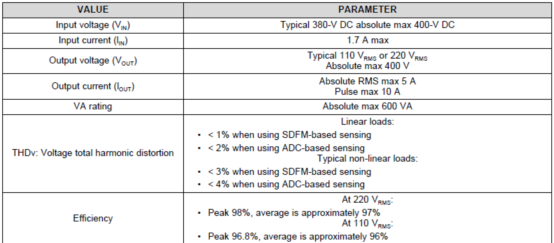

图. 参考设计TIDM-HV-1PH-DCAC概述图
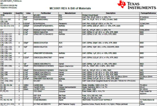
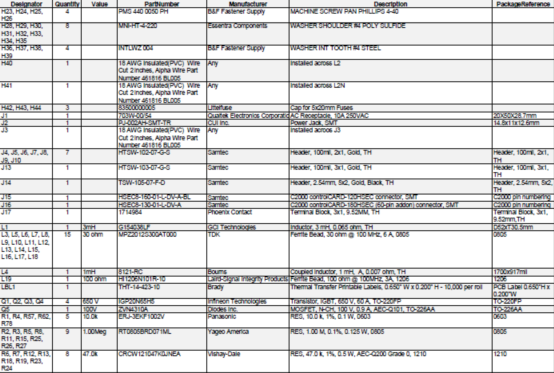
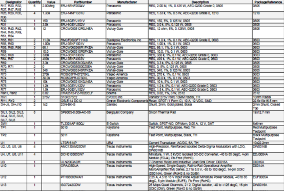
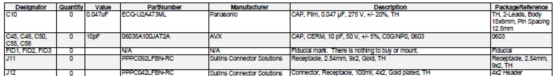
参考设计TIDM-HV-1PH-DCAC材料清单:
责任编辑:HanFeng
【免责声明】
1、本文内容、数据、图表等来源于网络引用或其他公开资料,版权归属原作者、原发表出处。若版权所有方对本文的引用持有异议,请联系拍明芯城(marketing@iczoom.com),本方将及时处理。
2、本文的引用仅供读者交流学习使用,不涉及商业目的。
3、本文内容仅代表作者观点,拍明芯城不对内容的准确性、可靠性或完整性提供明示或暗示的保证。读者阅读本文后做出的决定或行为,是基于自主意愿和独立判断做出的,请读者明确相关结果。
4、如需转载本方拥有版权的文章,请联系拍明芯城(marketing@iczoom.com)注明“转载原因”。未经允许私自转载拍明芯城将保留追究其法律责任的权利。
拍明芯城拥有对此声明的最终解释权。
相关资讯
:
基于MC33771主控芯片的新能源锂电池管理系统解决方案

AMIC110 32位Sitara ARM MCU开发方案

基于AMIC110多协议可编程工业通信处理器的32位Sitara ARM MCU开发方案

基于展讯SC9820超低成本LTE芯片平台的儿童智能手表解决方案

基于TI公司的AM437x双照相机参考设计

基于MTK6580芯片的W2智能手表解决方案


 2012- 2022 拍明芯城ICZOOM.com 版权所有 客服热线:400-693-8369 (9:00-18:00)


