


 产品分类
产品分类
On Semi CP51705单路6ASiC MOSFET驱动方案
 207
207
 拍明
拍明
原标题:On Semi CP51705单路6ASiC MOSFET驱动方案
On Semi公司的CP51705是单路6A高速低边SiC MOSFET驱动器,源电流和沉电流6A,为了获得最低的导通损耗,驱动器能对SiC MOSFET提供最大限度的栅极电压,主要用在驱动SiC MOSFET器件,工业逆变器,马达驱动器以及PFC,AC/DC转换器和DC/DC转换器.本文介绍了CP51705主要特性,框图和应用电路,以及评估板EVBUM2528/D,电路图,材料清单和PCB设计图.
The NCP51705 driver is designed to primarily drive SiC MOSFETtransistors. To achieve the lowest possible conduction losses, thedriver is capable to deliver the maximum allowable gate voltage to theSiC MOSFET device. By providing high peak current during turn−onand turn−off, switching losses are also minimized. For improvedreliability, dV/dt immunity and even faster turn−off, the NCP51705can utilize its on−board charge pump to generate a user selectablenegative voltage rail.
For full compatibility and to minimize the complexity of the biassolution in isolated gate drive applications the NCP51705 alsoprovides an externally accessible 5 V rail to power the secondary sideof digital or high speed opto isolators.
The NCP51705 offers important protection functions such asunder−voltage lockout monitoring for the bias power and thermalshutdown based on the junction temperature of the driver circuit.
CP51705主要特性:
• High Peak Output Current with Split Output Stages to allowindependent Turn−ON/Turn−OFF Adjustment;
♦ Source Capability: 6 A
♦ Sink Capability: 6 A
• Extended Positive Voltage Rating for Efficient SiC MOSFETOperation during the Conduction Period
• User−adjustable Built−in Negative Charge Pump for Fast Turn−offand Robust dV/dt Immunity
• Accessible 5 V Reference / Bias Rail for Digital Oscillator Supply
• Adjustable Under−Voltage Lockout
• Desaturation Function
• Thermal Shutdown Function (TSD)
• Small & Low Parasitic Inductance QFN24 Package
CP51705典型应用:
• Driving SiC MOSFET
• Industrial Inverters, Motor Drivers
• PFC, AC to DC and DC to DC Converters
NCP51705 SiC评估板EVBUM2528/D
This document describes the use and applications for theNCP51705 SiC driver mini EVB. The EVB is designed ona four layer PCB and includes the NCP51705 driver and allthe necessary drive circuitry. The EVB also includes anon−board digital isolator and the ability to solder anyMOSFET or SiC MOSFET in a T0247 high voltagepackage. The EVB does not include a power stage and isgeneric from the point of view that it is not dedicated to anyparticular topology. It can be used in any low−side orhigh−side power switching application. For bridgeconfigurations two or more of these EVBs can be configuredin a totem pole type drive configuration. The EVB can beconsidered as an isolator+driver+T0247 discrete module.
外形图")
图.评估板EVBUM2528/D(35 mm x 15 mm x 5 mm)外形图
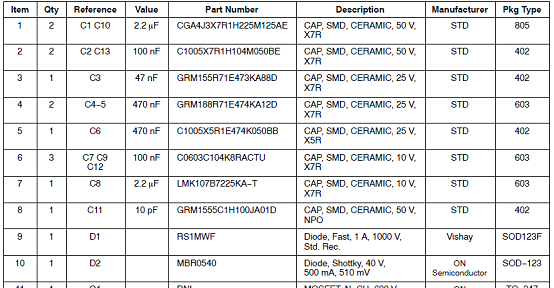
评估板EVBUM2528/D材料清单:

详情请见:
责任编辑:HanFeng
【免责声明】
1、本文内容、数据、图表等来源于网络引用或其他公开资料,版权归属原作者、原发表出处。若版权所有方对本文的引用持有异议,请联系拍明芯城(marketing@iczoom.com),本方将及时处理。
2、本文的引用仅供读者交流学习使用,不涉及商业目的。
3、本文内容仅代表作者观点,拍明芯城不对内容的准确性、可靠性或完整性提供明示或暗示的保证。读者阅读本文后做出的决定或行为,是基于自主意愿和独立判断做出的,请读者明确相关结果。
4、如需转载本方拥有版权的文章,请联系拍明芯城(marketing@iczoom.com)注明“转载原因”。未经允许私自转载拍明芯城将保留追究其法律责任的权利。
拍明芯城拥有对此声明的最终解释权。
相关资讯
:
基于MC33771主控芯片的新能源锂电池管理系统解决方案

AMIC110 32位Sitara ARM MCU开发方案

基于AMIC110多协议可编程工业通信处理器的32位Sitara ARM MCU开发方案

基于展讯SC9820超低成本LTE芯片平台的儿童智能手表解决方案

基于TI公司的AM437x双照相机参考设计

基于MTK6580芯片的W2智能手表解决方案


 2012- 2022 拍明芯城ICZOOM.com 版权所有 客服热线:400-693-8369 (9:00-18:00)


