


 产品分类
产品分类
ADI ADuCM355智能电子化学传感器接口解决方案
 359
359
 拍明
拍明
原标题:ADI ADuCM355智能电子化学传感器接口解决方案
ADI公司的ADuCM355是新一代智能电子化学传感器的新型传感器接口IC,能够在单个芯片上同时实现恒电位仪和电化学阻抗频谱分析仪(EIS)功能的唯一解决方案.器件集成了行业最先进的传感器诊断技术,具有卓越的低噪声和低功耗性能,并且尺寸最小,显著节约成本.主要用在工业气体检测,仪器仪表,生命体征监测和疾病管理等.本文介绍了ADuCM355主要特性,功能框图,应用电路以及评估板EVAL-ADuCM355QSPZ主要特性和应用连接图.
The ADuCM355 is an on-chip system designed to control andmeasure electrochemical and biosensors. The ADuCM355 is an ultralow power mixed-signal microcontroller based on theARMRCortex™-M3 processor. It is designed with current, voltage, and impedance measurement capability. The ADuCM355 features a 16-bit, 400 kSPS multichannel successive approximation register (SAR) analog-to-digitalconverter (ADC) with input buffers, built in antialias filter(AAF) and programmable gain amplifier (PGA). The current inputs include three transimpedance amplifiers (TIA) with programmable gain and load resistors for measuring differentsensor types. The analog front end (AFE) also contains twomore low power amplifiers designed specifically for potentiostat capability to maintain a constant bias voltage to an external electrochemical sensor. The noninverting inputs of these twoamplifiers are controlled by on-chip dual output digital-to-analog converters (DAC). The analog outputs include anotherhigh speed DAC and output amplifier designed to generate an ac signal. The ADC is capable of operating at conversion rates up to 400 kSPS with an input range of ±0.9 V. An input mux before the ADC allows the user to select an input channel formeasurement. These input channels include three externalcurrent inputs, multiple external voltage inputs, and internal channels. The internal channels allow diagnostic measurementsof the internal supply voltages, die temperature, and referencevoltages. Two of the three voltage DACs are dual output, 12-bit stringDACs. One output per DAC controls the noninverting input of a potentiostat amplifier, and the other controls the noninverting input of the TIA.
The third DAC (sometimes referred to as the high speed DAC)is designed for the high power TIA for impedancemeasurements. Its output frequency range is up to 200 kHz. A precision 1.82 V and 2.5 V on-chip reference source is available. The internal ADC and VDAC circuits use this on-chip reference source to ensure low drift performance for all of these peripherals.
The ADuCM355 integrates a 26 MHz ARM Cortex-M3processor. It is a 32-bit reduced instruction set computer (RISC) machine, offering up to 32.5 DMIPS peak performance. The ARM Cortex-M3 processor also has a flexible multichannel direct memory access controller (DMA) supporting serial peripheral interface (two independent SPI ports), universalasynchronous receiver/transmitter (UART), and I2Ccommunication peripherals. The ADuCM355 has 128 kB of nonvolatile flash/EE memory and 64 kB of SRAM integrated on-chip. The digital processor subsystem is clocked from a 26 MHz on-chip oscillator. This is the source of the main digital die systemclock. Optionally, a 26 MHz PLL can be used as the digitalsystem clock. This clock can be internally subdivided so that the processor operates at a lower frequency and saves power. A lowpower internal 32 kHz oscillator is available and can clock thetimers. The ADuCM355 includes three general-purpose timers,a wake-up timer (which can be used as a general-purposetimer), and a system watchdog timer. The analog subsystem has a separate 16 MHz oscillator used to clock the ADC, DACs, and other digital logic on the analog die.
The analog die also contains a separate 32 kHz, low poweroscillator to clock a watchdog timer on the low voltage die. Both the 32 kHz oscillator and this watchdog are independent from the digital die oscillators and system watchdog timer. A range of communication peripherals can be configured asrequired in a specific application. These peripherals includeUART, I2C, 2xSPI, and GPIO ports. The GPIO, combined with the general-purpose timers, can be combined to generate apulse width modulation (PWM) type output. On-chip factory firmware supports in-circuit erasing of user flashtriggered via the UART, while nonintrusive emulation and programdownload are supported via the serial wire debug port (SW-DP) interface. The ADuCM355 operates from 2.8 V to 3.6 V supply and isspecified over a temperature range of −40℃ to +85℃. The chip is packaged in a 72-lead 6 mm × 5 mm land grid array (LGA)package.
ADuCM355主要特性:
Analog input/output
16-bit, 400 kSPS ADC
Voltage, current, and impedance measurement capability
Internal/external current and voltage channels
Ultralow leakage switch matrix and input mux
Input buffers, programmable gain amplifier
Voltage DACs
2 dual output VDACs Output range 0.2 V to 2.4 V (±2.2 V voltage potential to sensor)
2 bias potentiostat and TIA amplifiers
Ultralow power, 1 μA per DAC
One high speed 12-bit VDAC
Output range to sensor ±607 mV
High speed TIA for impedance measurements
Programmable gain amplifier on output
Amplifiers, accelerators, and references 2 low power, low noise amplifiers
Suitable for potentiostat bias in electrochemical sensing
2 low power, low noise TIAs Suitable for measuring sensor current output 200 pA to 3 mA range Programmable load and gain resistors Analog hardware accelerators DDS waveform generator
DFT and digital filters 2.5 V and 1.82 V on-chip, precision voltage references Internal temperature sensor, ±2℃ accurate
Impedance measurement range of <1 Ω to 10 MΩ, 1 Hz to 200 kHz
Voltammetry scan rate up to 2000 steps per second
Microcontroller
26 MHz ARM Cortex-M3 processor
Serial wire port supports code download and debug
128 kB flash/64 kB of SRAM
Security/safety
Hardware crypto accelerator with AES-128 and AES-256
Hardware CRC with programmable polynomial generator Read/write protection of user flash
On-chip peripherals
UART, I2C, and SPI serial input/output
Up to 10 GPIO pins
External interrupt option
General-purpose, wake-up, and watchdog timers
Power
2.8 V to 3.6 V supply and active measurement range
Power-supply monitor
Active current consumption 30 μA/MHz for digital part
Hibernate with bias to external sensor, 8.5 μA
Shutdown mode with no SRAM retention, 2 μA
Packages and temperature range
6 mm × 5 mm, 72-lead LGA package
Fully specified for −40℃ to +85℃ ambient operation
ADuCM355应用:
Gas detection Food quality
Environmental sensing (air, water, soil)
Blood glucose meters
Life sciences and biosensing analysis
Bioimpedance measurements
General Amperometry, voltammetry, and impedance
spectroscopy functions
评估板EVAL-ADuCM355QSPZ
The ADuCM355 system on a chip provides the features needed to bias and measure a range of different electrochemical sensors. The EVAL-ADuCM355QSPZ allows users to evaluate the performance of the ADuCM355 when implementing a range of different electrochemical techniques, including chronoam-perometry, voltammetry, and electrochemical impedance spectroscopy (EIS).
评估板EVAL-ADuCM355QSPZ主要特性:
Debug/programming capability of ADuCM355
Evaluation capability with electrochemical gas sensors
ADT7420 0.5 C accurate temperature sensor via I2C
USB power option and connection to PC
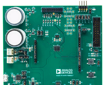
图.评估板EVAL-ADuCM355QSPZ外形图
详情请见:
责任编辑:HanFeng
【免责声明】
1、本文内容、数据、图表等来源于网络引用或其他公开资料,版权归属原作者、原发表出处。若版权所有方对本文的引用持有异议,请联系拍明芯城(marketing@iczoom.com),本方将及时处理。
2、本文的引用仅供读者交流学习使用,不涉及商业目的。
3、本文内容仅代表作者观点,拍明芯城不对内容的准确性、可靠性或完整性提供明示或暗示的保证。读者阅读本文后做出的决定或行为,是基于自主意愿和独立判断做出的,请读者明确相关结果。
4、如需转载本方拥有版权的文章,请联系拍明芯城(marketing@iczoom.com)注明“转载原因”。未经允许私自转载拍明芯城将保留追究其法律责任的权利。
拍明芯城拥有对此声明的最终解释权。
相关资讯
:
基于MC33771主控芯片的新能源锂电池管理系统解决方案

AMIC110 32位Sitara ARM MCU开发方案

基于AMIC110多协议可编程工业通信处理器的32位Sitara ARM MCU开发方案

基于展讯SC9820超低成本LTE芯片平台的儿童智能手表解决方案

基于TI公司的AM437x双照相机参考设计

基于MTK6580芯片的W2智能手表解决方案


 2012- 2022 拍明芯城ICZOOM.com 版权所有 客服热线:400-693-8369 (9:00-18:00)


