


 产品分类
产品分类
基于IDT公司的5L35023VersaClock 3S可编时钟发生器解决方案
 247
247
 拍明
拍明
原标题:IDT 5L35023VersaClock 3S可编时钟发生器解决方案
IDT公司的5L35023是VersaClock® 3S可编时钟发生器,1.8V工作,采用3 PLL架构,每个PLL可单独可编程,允许有多达6个频率输出,内置主动省功耗特性(PPS),性能-功耗平衡(PPB),降过冲技术(ORT)和极低功耗DCO以及动态频率控制(DFC),扩展频谱时钟有更低的系统EMI,I2C接口,主要用在嵌入计算设备,替代消费类应用晶振,以及SmartDevice,手持设备和消费类电子.本文介绍了5L35023主要特性,输出指标,框图以及5L35023 USB开发板主要功能布局和电路图.
The 5L35023 is a member of the VersaClock® 3S programmableclock generator family with 1.8V operation voltage, and isdesigned for industrial, consumer, and PCI Express applications.The device features a 3 PLL architecture design; each PLL isindividually programmable and allowing up to 6 unique frequencyoutputs.
The 5L35023 has built-in features such as Proactive PowerSaving (PPS), Performance-Power Balancing (PPB), OvershotReduction Technology (ORT) and extreme low power DCO. Aninternal OTP memory allows the user to store the configuration inthe device without programming after power-up, then program the5L35023 again through the I2C interface.
The device has programmable VCO and PLL source selection,allowing power-performance optimization based on the applicationrequirements.
5L35023主要特性:
▪ Configurable OE pin function as OE, PD#, PPS or DFC controlfunction
▪ Configurable PLL bandwidth; minimizes jitter peaking
▪ PPS: Proactive Power Saving features save power during theend device power down mode
▪ PPB: Performance Power Balancing feature allows minimumpower consumption based on required performance
▪ DFC: Dynamic Frequency Control feature allows user todynamically switch between and up to 4 different frequenciessmoothly
▪ Spread spectrum clock to lower system EMI
▪ I2C interface
▪ Suspend Mode, featuring RTC clock only when system goesinto low-power operation modes
5L35023主要指标:
▪ PCIe Gen1/2/3 compliant
▪ Typical 1.5ps rms jitter integer range: 12kHz–20MHz
▪ Typical ultra-power-down current 50μA
▪ < 2μA RTC clock in Suspend Mode operation
5L35023输出特性:
▪ 2 DIFF outputs with configurable LPHSCL, LVCMOS outputpairs: 1MHz–125MHz
▪ 3 LVCMOS outputs: 1MHz–125MHz
▪ LVPECL, LVDS, CML and SSTL logic can be easily supportedwith the LP-HCSL outputs. See application note AN-891 foralternate terminations
▪ Maximum of 8 LVCMOS outputs
▪ Low-power 32.768kHz clock supported for all SE1–SE3
5L35023典型应用:
▪ Embedded computing devices
▪ Consumer application crystal oscillator replacements
▪ SmartDevice, Handheld, and Consumer applications
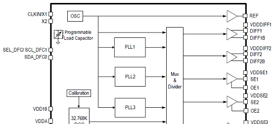
图1.5L35023框图
5L35023 USB开发板
The USB development kit board is ready with all of the necessary components and connections to test the functionality of theconfiguration.
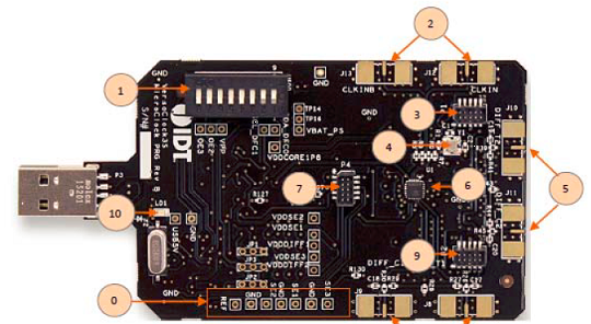
图2.5L35023 USB开发板外形和描述图
5L35023 USB开发板描述图:

详情请见:
![]() IDT_VC3S-5X3502X-DevKit-UserManual_MAE_20170705.pdf
IDT_VC3S-5X3502X-DevKit-UserManual_MAE_20170705.pdf
责任编辑:Davia
【免责声明】
1、本文内容、数据、图表等来源于网络引用或其他公开资料,版权归属原作者、原发表出处。若版权所有方对本文的引用持有异议,请联系拍明芯城(marketing@iczoom.com),本方将及时处理。
2、本文的引用仅供读者交流学习使用,不涉及商业目的。
3、本文内容仅代表作者观点,拍明芯城不对内容的准确性、可靠性或完整性提供明示或暗示的保证。读者阅读本文后做出的决定或行为,是基于自主意愿和独立判断做出的,请读者明确相关结果。
4、如需转载本方拥有版权的文章,请联系拍明芯城(marketing@iczoom.com)注明“转载原因”。未经允许私自转载拍明芯城将保留追究其法律责任的权利。
拍明芯城拥有对此声明的最终解释权。
相关资讯
:
基于MC33771主控芯片的新能源锂电池管理系统解决方案

AMIC110 32位Sitara ARM MCU开发方案

基于AMIC110多协议可编程工业通信处理器的32位Sitara ARM MCU开发方案

基于展讯SC9820超低成本LTE芯片平台的儿童智能手表解决方案

基于TI公司的AM437x双照相机参考设计

基于MTK6580芯片的W2智能手表解决方案


 2012- 2022 拍明芯城ICZOOM.com 版权所有 客服热线:400-693-8369 (9:00-18:00)


