


 产品分类
产品分类
基于Maxim公司的MAX98357A PCM输入D类音频放大器解决方案
 276
276
 拍明
拍明
原标题:Maxim MAX98357A PCM输入D类音频放大器解决方案
Maxim公司的MAX98357A/MAX98357B是数字脉码调制(PCM)输入D类放大器,提供AB类音频性能和D类效率,有五个可选择的增益设定(3dB, 6dB, 9dB, 12dB和15dB),单电源2.5V-5.5V工作,5V 4Ω时的输出功率为3.2W,效率92% (RL = 8Ω, POUT = 1W),输出噪音25μVRMS (AV = 15dB),1kHz时的THD+N为0.015%,主要用在笔记本电脑和上网本(Netbook),手机和平板电脑.本文介绍了MAX98357A/MAX98357B主要特性,功能框图和几种应用电路,以及MAX98357开发板DEV(WLP)主要特性,框图,电路图,材料清单和PCB设计图.
The MAX98357A/MAX98357B are digital pulse-code modulation (PCM) input Class D power amplifiers that provide Class AB audio performance with Class D efficiency. These ICs offer five selectable gain settings (3dB, 6dB, 9dB, 12dB, and 15dB) in I2S/left-justified mode set by a single gain select input and a fixed 12dB gain in TDM mode.
The digital audio interface is highly flexible with the MAX98357A supporting I2S data and the MAX98357B supporting left-justified data. Both ICs support 8 channel time division multiplexed (TDM) data. The digital audio interface accepts specified sample rates between 8kHz and 96kHz for all supported data formats. The ICs can be configured to produce a left channel, right channel, or (left/2 + right/2) output from the stereo input data. The ICs operate using 16/24/32-bit data for I2S and left-justified modes as well as 16-bit or 32-bit data using TDM mode. The ICs eliminate the need for the external MCLK signal that is typically used for PCM communication. This reduces EMI and possible board coupling issues in addition to reducing the size and pin count of the ICs.
The ICs also feature a very high wideband jitter tolerance (12ns typ) on BCLK and LRCLK to provide robust operation.Active emissions-limiting, edge-rate limiting, and overshoot control circuitry greatly reduce EMI. A filterless spread-spectrum modulation scheme eliminates the need for output filtering found in traditional Class D devices and reduces the component count of the solution.
The ICs are available in 9-pin WLP (1.345mm x 1.435mm x 0.64mm) and 16-pin TQFN (3mm x 3mm x 0.75mm) packages and are specified over the -40 ℃ to +85℃ temperature range.
MAX98357A/MAX98357B主要特性:
Single-Supply Operation (2.5V to 5.5V)
3.2W Output Power into 4Ω at 5V
2.4mA Quiescent Current
92% Efficiency (RL = 8Ω, POUT = 1W)
25μVRMS Output Noise (AV = 15dB)
Low 0.015% THD+N at 1kHz
No MCLK Required
Sample Rates of 8kHz to 96kHz
Supports Left, Right, or (Left/2 + Right/2) Output
Sophisticated Edge Rate Control Enables Filterless Class D Outputs
77dB PSRR at 1kHz
Low RF Susceptibility Rejects TDMA Noise from GSM Radios
Extensive Click-and-Pop Reduction Circuitry
Robust Short-Circuit and Thermal Protection
Available in Space-Saving Packages: 1.345mm x 1.435mm WLP (0.4mm Pitch) and 3mm x 3mm TQFN
MAX98357A/MAX98357B应用:
Notebook and Netbook Computers
Cellular Phones
Tablets

图1.MAX98357A/MAX98357B功能框图

图2.MAX98357A/MAX98357B增益6dB左路PCM工作电路

图3.MAX98357A/MAX98357B增益12dB左路PCM工作电路

图4.MAX98357A/MAX98357B增益6dB右路PCM工作电路
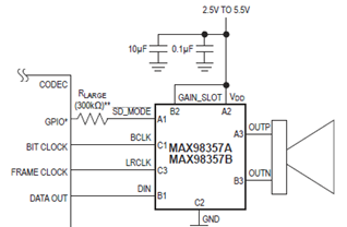
图5.MAX98357A/MAX98357B增益6dB(左路/2+右路/2)PCM工作电路

图6.MAX98357A/MAX98357B采用两个IC的立体声PCM工作电路

图7.MAX98357A/MAX98357B增益12dB通路TDM工作电路
MAX98357开发板DEV(WLP)
The MAX98357 development board (DEV board) is a fullyassembled and tested PCB that evaluates the MAX98357I2S digital input Class D power amplifier. The DEV boardoperates from a single 2.5V to 5.5V DC power supply andis capable of delivering 3.2W into a 4Ω load. The deviceoutputs can be connected directly to a speaker load forfilterless applications. However, a filter can be added toease evaluation. The MAX98357A accepts standard I2Sdata and the MAX98357B accepts left-justified digital audio data. Both versions also support 8-channel TDMaudio data.
The MAX98357 evaluation system (EV system) includesthe MAX98357 DEV board and Maxim Integrated’s audiointerface board (AUDINT001 board).
The AUDINT001 board provides an easy-to-use USBaudio-to-I2S converter. This allows for any computer tobecome a digital audio source, which can be used toevaluate the devices. The AUDINT001 board can also beused to power the MAX98357. This allows for a completeevaluation from a single USB connection.
MAX98357开发板DEV(WLP)主要特性:
●● 2.5V to 5.5V Single-Supply Operation
●● Only a Single External Component (VDD Capacitor)Required in Many Applications
●● I2S, Left-Justified, or TDM Input
●● Five Selectable Gains (3db, 6dB, 9dB, 12dB, and15dB)
●● Audio Channel Select (Left, Right, and Mono Mix)
●● Filterless Operation
●● Optional Class D Output Filters for Ease ofEvaluation
●● Proven PCB Layout
●● Fully Assembled and Tested
MAX98357开发板DEV(WLP)材料清单:

详情请见:
![]() MAX98357DEV_WLP-MAX98357EVSYS_WLP.pdf
MAX98357DEV_WLP-MAX98357EVSYS_WLP.pdf
责任编辑:Davia
【免责声明】
1、本文内容、数据、图表等来源于网络引用或其他公开资料,版权归属原作者、原发表出处。若版权所有方对本文的引用持有异议,请联系拍明芯城(marketing@iczoom.com),本方将及时处理。
2、本文的引用仅供读者交流学习使用,不涉及商业目的。
3、本文内容仅代表作者观点,拍明芯城不对内容的准确性、可靠性或完整性提供明示或暗示的保证。读者阅读本文后做出的决定或行为,是基于自主意愿和独立判断做出的,请读者明确相关结果。
4、如需转载本方拥有版权的文章,请联系拍明芯城(marketing@iczoom.com)注明“转载原因”。未经允许私自转载拍明芯城将保留追究其法律责任的权利。
拍明芯城拥有对此声明的最终解释权。
相关资讯
:
基于MC33771主控芯片的新能源锂电池管理系统解决方案

AMIC110 32位Sitara ARM MCU开发方案

基于AMIC110多协议可编程工业通信处理器的32位Sitara ARM MCU开发方案

基于展讯SC9820超低成本LTE芯片平台的儿童智能手表解决方案

基于TI公司的AM437x双照相机参考设计

基于MTK6580芯片的W2智能手表解决方案


 2012- 2022 拍明芯城ICZOOM.com 版权所有 客服热线:400-693-8369 (9:00-18:00)


