


 产品分类
产品分类
基于ADS58C48四路200MSPS设计的11位模数转换技术设计方案
 86
86
 拍明
拍明
原标题:基于ADS58C48四路200MSPS设计的11位模数转换技术设计方案
一、引言
随着高速数据采集技术在雷达、通信、电子测量以及仪器仪表等领域的广泛应用,如何在高速采样(200MSPS)条件下实现高精度(11位有效分辨率)的模数转换系统成为工程技术人员关注的重点。ADS58C48作为一款四通道高速模数转换器,其具有极低的采样延迟、优异的动态性能和较高的集成度,适合用于高密度、多通道数据采集系统。本文方案基于ADS58C48器件,结合高精度时钟、模拟前端电路、数字数据处理与校正技术,提出一套完整的11位模数转换技术实现方案,内容涉及元器件选型、功能分析、系统框图设计及电路实现细节,旨在为工程人员提供一个具有参考意义的设计范例。

二、技术指标与系统要求
在本设计方案中,主要技术指标和系统要求如下:
采样速率要求
ADS58C48提供四路通道,每路最高可达200MSPS的采样率,要求整个系统能保持稳定的高速采样能力。
有效分辨率要求
实现系统11位有效分辨率。虽然ADS58C48本身在高速下可能以较低位数采样,但通过多路数据融合、过采样及数字滤波校正技术,可实现11位有效分辨率。
通道数量及同步要求
四路并行采样通道要求各通道之间的采样时钟同步,保证多通道数据采集的时序一致性和相位匹配。
动态性能指标
信噪比(SNR)、失真指标(THD)、互调失真(IMD)等需满足高速ADC系统要求;
抗混叠性能要求高,前端滤波电路必须具备严格的带宽控制。
系统稳定性与抗干扰性
模拟前端设计需保证低噪声、高线性,同时在PCB布局和供电设计上需防止高速信号串扰、地回路干扰等问题。
系统接口要求
高速数据传输接口(如LVDS或串行高速链路)与后端FPGA或DSP数据处理单元对接,保证数据完整性;
配置、控制接口需实现灵活参数设置及在线校正功能。
温度补偿与校准功能
系统设计中应包含温度补偿及自校正算法,以补偿因温度漂移带来的偏移和增益误差。
三、系统总体架构设计
整个系统总体架构可划分为以下几个部分:
信号采集与模拟前端
模拟信号经输入缓冲、抗混叠滤波、可选放大后传递给ADC。前端设计需保证信号带宽、抑制杂散以及对高速信号的完整传输。
ADS58C48模数转换模块
四路高速ADC模块负责将模拟信号以200MSPS的速率进行采样,并输出数字信号。为提高分辨率,系统采用多路数据融合与数字校正技术。
时钟系统模块
高速、低抖动的参考时钟是实现高速采样的关键。时钟模块通常由低噪声振荡器、分频器和PLL构成,保证所有ADC及后端处理器的同步工作。
数字数据处理单元
数据采集后通过FPGA或高速DSP进行数据缓存、实时滤波、校正及数据重构,最终输出11位精度的数字信号。数据处理单元还负责实现通信接口,与上位机或其他控制器交换数据。
供电与参考电压系统
为保证高速采样和低噪声性能,系统中采用独立、低噪声的电源模块和精密参考电压源,确保ADC及模拟前端电路的稳定供电。
系统控制与校正模块
包括微控制器或FPGA内部的软件控制系统,实时监测系统状态、调节参数并进行在线校正,实现自适应优化。
下图给出了系统总体框图示意:


图中各模块之间通过高速信号线和控制总线相互连接,整个系统实现了从模拟信号采集、数据转换、实时数字信号处理到系统控制的完整流程。
四、关键模块设计
4.1 模拟前端电路设计
4.1.1 信号输入与缓冲
在高速ADC系统中,输入信号的完整性对最终转换精度影响巨大。采用低噪声、高带宽的缓冲放大器作为输入级,确保输入信号不受后续电路负载影响。可选器件包括ADI的AD8138、Texas Instruments的THS4509等高速差分放大器。
选择理由:
AD8138:具有低噪声、低失真、宽带宽(600MHz以上)以及较高的共模抑制比,非常适合于高速数据采集系统。
THS4509:作为射频前端放大器,能够提供低噪声、高增益及高速动态范围,对抗高速采样信号失真具有良好效果。
4.1.2 抗混叠滤波器设计
为了防止输入信号中高频分量混入采样带宽,设计一个低通抗混叠滤波器是必不可少的。滤波器一般选用无源RC或LC网络,结合精密电容、电感及电阻构成。例如可以采用Murata或TDK系列的高稳定性电容、电感元件。
设计要点:
带宽设定在采样频率的一半以内(例如设置截止频率在80~90MHz左右),
滤波器阶数需根据系统带宽和陡峭度要求确定(通常采用二阶或三阶Butterworth滤波器)。
4.2 ADS58C48模数转换模块
ADS58C48为四通道高速ADC,其核心性能指标包括:
采样速率: 每通道可达200MSPS
分辨率: 虽然器件本身可能在高速下为8~10位,但通过内部校正及数据后处理,可达到11位有效分辨率
接口方式: 支持LVDS输出,便于与高速数字处理器对接
在设计中,ADS58C48作为数据采集核心模块,其工作稳定性、时序同步性、数据传输完整性是整个系统性能的关键。为确保器件性能,设计中还需特别关注时钟、供电及PCB布局等因素。
4.3 时钟系统设计
高速ADC系统对时钟源要求极高,时钟抖动直接影响采样精度。设计中建议采用以下措施:
低抖动振荡器
推荐器件:SiTime、Crystek或Analog Devices的低相位噪声振荡器。
选择理由:高稳定性、低抖动特性,能够满足200MSPS及后续信号处理要求。
支持温度补偿,确保在环境温度变化时依然保持稳定的时钟输出。
分频及PLL模块
利用PLL技术对振荡器输出进行分频和整形,保证各模块之间的时钟同步。推荐选用具有低抖动和高稳定性的时钟分配器,例如TI的LMK04828。
功能说明:将参考时钟分频并分配到各个采样、数据处理模块,确保全系统时钟一致性。
内部集成的PLL可根据系统需求调整时钟频率,满足多通道同步要求。
4.4 电源与参考电压系统设计
电源和参考电压对高速ADC系统的噪声性能及稳定性至关重要。系统中建议采用多级电源滤波与隔离技术,推荐方案如下:
电源管理模块
DC-DC转换器: 采用例如TI的LMZM23601模块,提供高效、低噪声的转换,同时保证多路输出稳压。
低噪声LDO稳压器: 推荐器件如TI的TPS7A4700、Analog Devices的ADM7150等,保证敏感模拟电路的供电纯净。
选择理由:这些器件具有低纹波、快响应、良好的负载调节特性,适合用于ADC、前端放大器等高精度模块。
参考电压模块
采用高精度、低温漂的参考电压源,例如ADI的ADR4520或Texas Instruments的REF5020。
功能说明:提供稳定的参考电压,确保ADC转换精度;
温漂低,长期稳定性好,适用于高精度数据采集场合。
4.5 数字数据处理单元设计
高速ADC采集的数据量巨大,数字数据处理单元主要承担数据缓存、融合、校正和高速接口等任务。设计中建议采用FPGA或高速DSP作为主控芯片。常用器件包括:
FPGA: 例如Xilinx Kintex-7、Altera Stratix系列等,具有高并行处理能力和丰富的高速接口资源。
高速缓存接口: 配合DDR3/DDR4内存或FIFO电路,实现数据的临时存储与缓冲,确保数据传输无丢失。
数据处理算法: 利用FPGA内部逻辑实现数字滤波、校正算法以及数据重构,通过内部IP核实现LVDS接口数据的采集与解码。
选择理由:
FPGA具有极高的数据处理速度和灵活性,能够实时处理200MSPS采样数据,并通过自校正算法提升系统有效分辨率。
通过硬件描述语言(HDL)实现的数字电路具备良好的可扩展性和稳定性,适合复杂数据采集系统的设计。
4.6 控制与通信接口设计
系统中需要一个灵活的控制接口,实现参数设置、状态监测以及校正指令下达。推荐采用SPI、I²C等标准接口,并配合专用MCU或FPGA内部软核。
推荐器件:
MCU可以选用STMicroelectronics的STM32系列或Microchip的PIC32系列,具有丰富外设接口和良好的软件生态。
控制接口电路设计上,需考虑抗干扰设计、接口电平匹配和时序要求,确保控制数据传输的可靠性。
五、元器件优选与详细说明
在整个设计方案中,每个模块的性能直接决定了系统整体的精度和稳定性。下面详细说明各主要元器件的型号选择、器件作用及选择理由。
5.1 ADS58C48高速ADC
器件型号: ADS58C48
主要参数: 四路通道、200MSPS采样速率、支持LVDS输出、低采样延迟
作用: 作为核心模数转换器,实现模拟信号的高速采样及数字化处理。
选择理由:
内部集成度高,能实现多通道同步采样;
数据转换速度快,满足高频信号采样要求;
支持后续通过数字处理实现11位有效分辨率,是实现高速高精度数据采集的理想选择。
5.2 模拟前端放大器
推荐器件型号: AD8138 或 TI THS4509
主要参数: 宽带宽(>600MHz)、低噪声、低失真、较高共模抑制比
作用: 对输入模拟信号进行前置缓冲和放大,同时提供差分信号驱动,保证信号质量。
选择理由:
AD8138具有非常低的噪声系数和出色的线性性能,非常适合高速信号预处理;
THS4509在高频信号放大方面表现优异,能够有效保证输入信号的动态范围。
5.3 抗混叠滤波器无源元件
推荐器件型号: 高精度、低温漂电容(例如Murata GRM系列)、低容差电阻及高品质电感(TDK系列)
主要参数: 高稳定性、低温漂、适合构成Butterworth或Chebyshev滤波网络
作用: 限制输入信号频带,抑制高频噪声及混叠失真,为ADC提供纯净采样信号。
选择理由:
高品质无源器件可以大大降低滤波器自身引入的噪声和温漂,保证信号滤波精度;
经过精密匹配后的滤波网络可以实现理想的截止特性,满足系统严格的抗混叠要求。
5.4 时钟振荡器及分频器
推荐器件型号:
振荡器:SiTime SiT5518系列或Crystek CVHD系列
分频器/时钟分配器:TI LMK04828
主要参数: 振荡器具备低相位噪声(低至几皮秒抖动)、高频率稳定性;分频器具有低抖动、精密时钟分配功能。
作用: 为整个系统提供高速、低抖动的参考时钟信号,确保各模块时序同步。
选择理由:
SiTime及Crystek系列在工业、通信领域已有广泛应用,具有极高的可靠性和稳定性;
LMK04828能够根据系统需求灵活分配时钟,同时降低时钟干扰,确保ADC采样精度。
5.5 电源管理模块
DC-DC转换器
推荐器件型号: TI LMZM23601
主要参数: 高效率、低噪声、支持多路输出
作用: 实现输入电压到各模块工作电压的高效转换,提供稳定电源。
选择理由: 高效率和低噪声是高速ADC系统的必备条件,LMZM23601在多路稳压输出上具有良好表现。
低噪声LDO稳压器
推荐器件型号: TI TPS7A4700 或 Analog Devices ADM7150
主要参数: 低纹波、快速负载响应、优秀的电压精度
作用: 为敏感模拟模块和参考电压电路提供纯净、稳定的电源。
选择理由: 低噪声LDO能有效滤除DC-DC转换器可能引入的噪声,保证ADC和前端电路的性能。
5.6 参考电压模块
推荐器件型号: ADI ADR4520 或 TI REF5020
主要参数: 高精度(误差低于0.05%)、低温漂(<10ppm/℃)
作用: 提供稳定的基准电压,保证ADC转换过程中的参考稳定性。
选择理由:
高精度参考电压是实现11位有效分辨率的关键,ADR4520和REF5020均具备出色的长期稳定性;
温漂低,能够在各种环境温度下保持稳定输出,为系统校正提供可靠基准。
5.7 FPGA/DSP数据处理单元
推荐器件型号: Xilinx Kintex-7 系列或Altera Stratix V 系列
主要参数: 高并行处理能力、大量高速I/O接口、内部高速缓存支持
作用: 实时接收ADS58C48输出的高速数据流,完成数据融合、数字滤波、校正和数据传输任务。
选择理由:
FPGA提供了灵活的硬件编程环境,能根据不同应用实现定制化数据处理;
高速数据接口保证了系统数据流的稳定传输,满足高速采集需求。
5.8 控制单元与通信接口
推荐器件型号: STM32F7系列(或其他高性能MCU,如PIC32)
主要参数: 多通道SPI/I²C接口、较高主频、丰富外设资源
作用: 实现系统参数配置、状态监控、在线校正指令下达及与上位机的数据交互。
选择理由:
STM32F7系列具备强大的处理能力和丰富的接口资源,适合高速控制和数据管理;
软件生态完善,开发调试方便,能实现复杂控制算法和实时状态反馈。
六、系统电路原理图及说明
为实现上述各模块之间的高效连接和协调工作,设计中将重点关注高速信号布线、功率与地平面隔离及EMI抑制。下图为系统整体电路框图及主要子模块示意图:


说明:
时钟系统: 由低噪振荡器输出信号经过PLL/分频后分发给ADC、FPGA及其他同步模块,保证全系统时序一致。
电源系统: 多级稳压电路(DC-DC转换器+低噪LDO)提供纯净电压,同时由高精度参考电压模块确保ADC转换基准稳定。
模拟前端: 输入信号经缓冲放大后进入抗混叠滤波器,滤除高频杂讯,输出经处理的模拟信号供ADC采样。
高速ADC模块: ADS58C48将四路模拟信号以200MSPS速率转换为数字信号,并通过LVDS接口输出至数据接口电路。
数字数据处理: FPGA/DSP单元接收高速数据,进行实时数据融合、数字滤波、校正处理后存储或通过控制接口传输至上位机。
控制接口: 系统管理模块通过标准通信接口实现对各模块的参数配置、状态监控及校正指令下达。
七、系统调试与校准方案
高速ADC系统在实际应用中往往受到元器件温漂、PCB走线、供电噪声等多重影响,故在设计中必须充分考虑调试与校准。具体方案包括:
7.1 现场调试流程
静态参数调试
检查电源、时钟、参考电压输出是否稳定;
测试各模块间接口连通性,确保无短路或干扰。
模拟前端信号调试
利用示波器及频谱仪检测缓冲放大器和抗混叠滤波器的输出波形;
调整放大器增益及滤波器截止频率,确保信号完整性。
ADC采样调试
在标准信号源下采集数据,利用逻辑分析仪观察LVDS数据时序;
调整采样时钟相位,确保各通道同步采样无数据偏移。
7.2 校准方案
数字校正算法
利用FPGA内置算法对ADC输出数据进行线性校正,补偿增益和偏置误差;
采用过采样与数字滤波技术,提高系统有效分辨率至11位。
温度补偿设计
在电路中增加温度传感器,通过MCU采集温度数据,实时调整校正参数;
利用预先建立的温漂模型,在线修正由温度变化带来的系统误差。
系统自检与在线校准
设计周期性校准程序,通过内置标准信号源自动检测系统状态,完成自检;
当检测到采样数据偏离标准时,系统自动调整内部校正参数,并反馈至上位机进行记录。
八、仿真与验证
在原理图设计完成后,采用电路仿真软件(如ADS、PSpice或Cadence)对关键电路进行仿真,主要验证以下内容:
信号前端仿真
模拟缓冲放大器与滤波器的传输函数,验证信号带宽与相位特性;
分析抗混叠滤波器在不同频率下的衰减效果,确保截止频率与设计指标吻合。
电源噪声仿真
分析DC-DC转换器及LDO稳压器在工作时的纹波及噪声谱,确保满足ADC对电源纯净度要求;
对PCB电源分布网络进行电磁干扰(EMI)仿真,优化滤波设计。
时钟系统仿真
验证振荡器和PLL电路的稳定性、相位噪声及抖动指标,确保满足200MSPS采样需求;
模拟时钟分配网络,检测各节点时钟一致性及延迟特性。
数字数据处理仿真
在FPGA开发平台上利用仿真工具(如ModelSim)对数据处理算法进行仿真,验证校正、滤波及数据融合效果;
对LVDS接口进行时序仿真,确保高速数据传输的完整性和稳定性。
九、系统实现与调试注意事项
在实际电路板设计和系统实现过程中,还需注意以下问题:
PCB布局设计
高速信号通道应采用差分走线,保证阻抗匹配;
模拟与数字地应分层设计,避免地回路干扰;
电源层与信号层之间应合理安排滤波及屏蔽,减少电磁干扰。
散热设计
高速ADC、FPGA及相关功率模块工作时发热较大,须在PCB上预留足够散热空间;
采用散热铜箔、散热片或风扇对关键器件进行主动或被动散热设计,确保长期稳定工作。
抗干扰设计
针对高频采样及数据传输,PCB设计中应严格控制串扰、反射及噪声问题;
对外部接口(如高速LVDS、SPI、I²C)增加适当的EMI屏蔽和滤波电路,防止外界干扰进入系统内部。
调试与测试接口
设计时预留测试点、调试接口(如JTAG、Probe点),便于在开发过程中对关键节点进行检测;
建立完善的测试流程,包括单板测试、系统级测试及环境适应性测试,确保各项指标满足设计要求。
十、系统性能评估与优化
在完成硬件调试及软件校正后,需对系统性能进行综合评估:
动态性能测试
通过施加标准正弦波信号,利用频谱仪检测SNR、SFDR、THD等指标,验证是否达到11位有效分辨率;
对比不同信号频率、幅度下的采样结果,分析系统的线性度及稳定性。
长期稳定性测试
在不同环境温度下测试系统采样数据,评估温漂对系统精度的影响;
实施长期连续采样测试,检测系统在长时间运行下的误差累积情况,并验证在线校正机制的有效性。
数据处理延迟与实时性
测试FPGA数据处理模块对高速数据流的实时处理能力,确保数据融合及校正运算在采样周期内完成;
分析LVDS传输链路时延及数据完整性,优化接口电路设计。
优化方案
根据测试结果,对模拟前端、时钟系统、供电模块等关键部分进行优化设计;
调整数字校正算法,进一步提升数据处理精度,实现系统性能的整体提升。
十一、总结
本文基于ADS58C48四路200MSPS高速ADC器件,设计了一套实现11位有效分辨率的模数转换系统方案。方案从系统总体架构、模拟前端设计、时钟与供电系统、电路板布局、数字数据处理及在线校正等多个角度进行了全面阐述。主要结论如下:
系统架构合理性
通过前端信号缓冲、抗混叠滤波及精密时钟、供电设计,实现了高速、低噪、高精度数据采集;
模数转换、数字数据处理及校正模块构成的整体架构,有效弥补了高速ADC器件在单次转换位数上的不足,通过后续数字处理实现了11位有效分辨率。
元器件优选关键性
ADS58C48作为核心采样器件,其高速采样能力为系统提供了坚实基础;
采用低噪声放大器、精密参考电压、低抖动时钟及高效电源管理模块,保证了系统整体的高精度与稳定性;
FPGA/DSP数据处理单元实现高速数据融合和校正,使系统在高速采样条件下达到高精度输出。
调试与优化措施
详细的调试流程和在线校正设计,有效抵消了因元器件温漂、PCB走线等因素引起的误差;
仿真与实测结合的方案验证,确保了系统各项指标均达到预期要求。
应用前景广阔
该设计方案适用于雷达、通信、仪器仪表等对高速、高精度数据采集要求较高的领域;
系统模块化设计便于后续升级和功能扩展,可根据不同应用场景进行定制化改进。
综上所述,本方案在理论设计、器件选型、电路实现和系统校准等方面均给出了详尽说明,为工程人员在高速ADC系统设计提供了一份较为完备的参考文档。
十二、参考文献与资料
ADS58C48器件数据手册及应用笔记(Texas Instruments官方文档);
高速ADC系统设计原理与应用(相关学术论文及专著);
模拟前端电路设计、抗混叠滤波器及高速PCB布局设计资料(ADI、TI技术文档);
时钟系统、低噪声振荡器及分频器应用设计(SiTime、Crystek及TI LMK04828数据手册);
FPGA数据处理与高速接口设计技术(Xilinx及Altera技术资料);
电源管理与参考电压模块设计(TI TPS7A4700、LMZM23601、ADR4520等器件应用笔记)。
附录:详细电路原理图说明
在实际工程中,为了便于生产调试,可将以上各模块详细分解为以下几个子电路:
时钟电路原理图
输入低噪振荡器模块输出经分频器及PLL模块,连接到各个高速模块的时钟输入端。
在关键节点处设计缓冲放大及电容滤波,保证时钟信号的完整性。
电源及参考电压电路
主电源经过DC-DC转换器转换为多路输出,分别供给模拟前端、ADC、FPGA及MCU。
在各电源输入端增加LC滤波器和EMI抑制电路,确保电源纯净;
精密参考电压模块直接连接至ADC参考端,并在周围布局屏蔽层以防干扰。
模拟前端电路图
信号输入经屏蔽连接到缓冲放大器(如AD8138),输出经过匹配阻抗的抗混叠滤波器后送入ADC通道。
布局上应保持差分信号路径的对称性,避免共模干扰和串扰问题。
ADC数据采集及数字接口电路图
ADS58C48的LVDS输出经过高速接收缓冲器传输至FPGA板卡;
在接口电路中设计必要的终端电阻匹配及阻抗调节,确保数据传输的稳定性。
FPGA内部设计专用IP核,实现数据校正、缓存及接口转换,后续通过SPI或Ethernet传输到上位机。
结语
本设计方案从需求分析、系统总体架构、关键模块详细设计、元器件优选、原理图设计、调试校准以及系统优化等多方面做了系统论述,充分考虑了高速采样、低噪声、信号完整性以及温度补偿等关键问题,旨在通过硬件与数字校正技术协同作用,实现基于ADS58C48的11位模数转换系统。该方案不仅适用于高速数据采集系统的研发,还为未来系统优化与新技术集成提供了良好的平台和思路。
希望本文提供的详尽设计思路、元器件选型依据及电路实现说明,能为相关领域工程师在实际项目中提供参考与借鉴。今后随着技术进步与新器件的不断出现,系统设计亦可在此基础上不断升级优化,以满足更高性能、更低功耗及更广泛应用场景的要求。
责任编辑:David
【免责声明】
1、本文内容、数据、图表等来源于网络引用或其他公开资料,版权归属原作者、原发表出处。若版权所有方对本文的引用持有异议,请联系拍明芯城(marketing@iczoom.com),本方将及时处理。
2、本文的引用仅供读者交流学习使用,不涉及商业目的。
3、本文内容仅代表作者观点,拍明芯城不对内容的准确性、可靠性或完整性提供明示或暗示的保证。读者阅读本文后做出的决定或行为,是基于自主意愿和独立判断做出的,请读者明确相关结果。
4、如需转载本方拥有版权的文章,请联系拍明芯城(marketing@iczoom.com)注明“转载原因”。未经允许私自转载拍明芯城将保留追究其法律责任的权利。
拍明芯城拥有对此声明的最终解释权。
相关资讯
: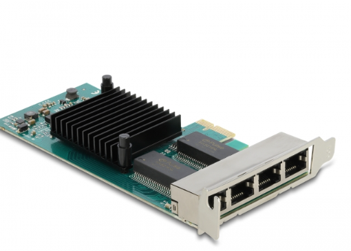
基于Xilinx XCKU115的半高PCIe x8 硬件加速卡设计方案
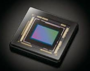
图像传感器在汽车、工业和边缘AI的应用动向
基于RFID技术的智能档案管理系统设计方案
如何确保工业物联网设计符合ISA/IEC安全标准
基于LPC55S69+i.MX 8M的快速灵活EV充电系统解决方案
如何利用物质连接智能家居自动化的孤岛


 2012- 2022 拍明芯城ICZOOM.com 版权所有 客服热线:400-693-8369 (9:00-18:00)


