基于EFM8UB11/Si5326/Si570/主控器件的光模块误码仪解决方案
 242
242
 拍明
拍明
概述
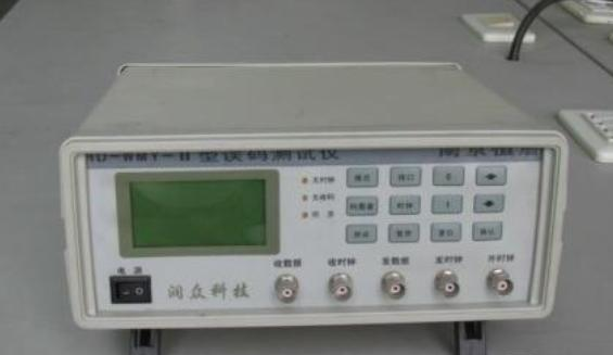
光模块专用测试误码仪主要利用PRBS发生模块,将高速PRBS信号发送给被测试光模块,之后将码流输出到误码接收检测模块,通过内部逻辑电路进行误码计算、统计,得出误码率。误码仪需要测试多种速率的光模块,因此传统误码仪设计客户可能会自己搭建锁相环(时钟发生器)或者使用大量单频点晶振作为时钟源,多颗晶振会占用大量PCB,而自行搭建的PLL,性能不稳定。本方案采用可编程晶振或多路时钟发生器,能以单芯片方案实现多种速率光模块的误码测试。
优势
· 8bit USB接口MCU(EFM8UB11)是一款集全速和低速低功耗USB外围接口的MCU,对于便携式设备,客户可直接使用该USB通信接口进行设计。
【EFM8UB11】
UG240: EFM8UB1-SLSTK2000A User's Guide
The EFM8UB1-SLSTK2000A is an excellent starting point to get familiar with the EFM8 EFM8UB1 Universal Bee microcontrollers.
The kit contains sensors and peripherals demonstrating some of the MCU's many capabilities.
The kit can also serve as a starting point for application development.
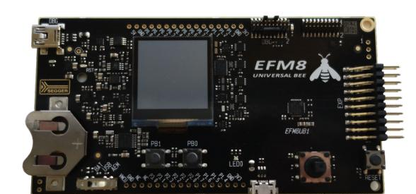
The kit includes the following:
• EFM8UB1 Universal Bee Starter Kit Board
• 1 x CR2032 battery
• Getting Started card
• 1 x mini and 1 x micro USB cables
KEY FEATURES
• EFM8UB10F16G MCU with 16 KB Flash and 2 KB RAM.
• 20-pin expansion header.
• Power sources include USB and CR2032 battery.
• 2 user buttons, 1 tri-color LED.
• 8-direction joystick.
• Ultra low power 128x128 pixel MemoryLCD.
1. Getting Started
Hardware
To set up the hardware for the EFM8UB1-SLSTK2000A kit:
1. Provide power to the board by connecting the USB connector to the PC using the provided USB cable.
2. Move the switch to the Advanced Energy Monitor (AEM) position.

Figure 1.1. Hardware Setup
Software
The first step to get started with your new EFM8UB1-SLSTK2000A is to go to
The Simplicity Studio software package contains all the tools, drivers, software examples and documentation needed to use the
EFM8UB1 Starter Kit. The board comes pre-loaded with a default application, Space Invaders, to interact with while the software downloads.
After downloading the latest version of Simplicity Studio and installing:
1. Select the J-Link adapter for the kit under [Devices].
2. Click one of the demos available under [Getting Started]>[Demos] or click the [Getting Started]>[Demos]>[View All] to view the
entire list of available demos.
3. Click the [Rainbow Blinky] demo and click [Start] to download and run the demo.
Additional demos showcasing the various features of the EFM8 are also available in Simplicity Studio.
2. Kit Block Diagram
An overview of the EFM8UB1 Starter Kit is shown in the figure below.
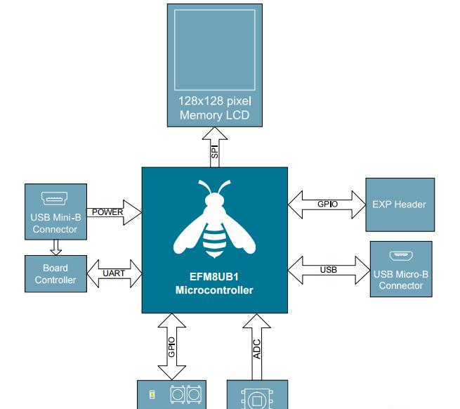
Figure 2.1. EFM8UB1-SLSTK2000A Block Diagram
3. Kit Hardware Layout
The layout of the EFM8UB1 Starter Kit is shown below.

Figure 3.1. EFM8UB1-SLSTK2000A Hardware Layout
Figure 3.1. EFM8UB1-SLSTK2000A Hardware Layout
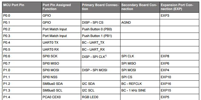
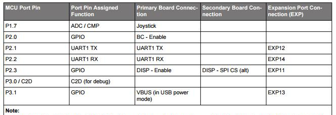
The EFM8 device on the kit is connected to several peripherals. The table below shows all of the external connections to the MCU.
Table 3.1. Kit MCU Connections
· 去抖时钟发生器(Si5326),内部采用DSPLL专利技术,在频率合成输出时能有效抑制输入时钟的抖动,低抖动时钟可以降低频率误差本身带来的通信误码率。
【 Si5326】
Description
The Si5326 is a jitter-attenuating precision clock multiplier forapplications requiring sub 1ps jitter performance. The Si5326accepts dual clock inputs ranging from 2kHz to 710MHz andgenerates two clock outputs ranging from 2kHz to 945MHzand select frequencies to 1.4GHz. The two outputs aredivided down separately from a common source. The deviceprovides virtually any frequency translation combinationacross this operating range. The Si5326 input clockfrequency and clock multiplication ratio are programmablethrough an I2C or SPI interface. The Si5326 is based onSilicon Laboratories' 3rd-generation DSPLL® technology,which provides any-rate frequency synthesis and jitterattenuation in a highly integrated PLL solution that eliminatesthe need for external VCXO and loop filter components. TheDSPLL loop bandwidth is digitally programmable, providingjitter performance optimization at the application level.Operating from a single 1.8, 2.5, or 3.3V supply, the Si5326is ideal for providing clock multiplication and jitter attenuationin high performance timing applications.
Features
Generates any frequency from 2kHz to 945MHz and select frequencies to 1.4GHz from an input frequency of 2kHz to 710MHz
Ultra-low jitter clock outputs w/jitter generation as lowas0.3psrms(50kHz–80MHz)
Integrated loop filter with selectable loop bandwidth (60Hzto8.4kHz)
Meets OC-192 GR-253-CORE jitter specifications
Dual clock inputs w/manual or automatically controlled hitless switching
Dual clock outputs with selectable signal format (LVPECL, LVDS, CML, CMOS)
Support for ITU G.709 and custom FEC ratios (255/238, 255/237, 255/236)
LOL, LOS, FOS alarm outputs
Digitally-controlled output phase adjust
I2C or SPI programmable
On-chip voltage regulator for 1.8, 2.5, or 3.3V
±10% operation
Small size: 6x6mm 36-lead QFN
Pb-free, ROHS compliant
Applications
SONET/SDH OC-48/OC-192 line cards
GbE/10GbE, 1/2/4/8/10GFC line cards
ITU G.709 and custom FEC line cards
Optical modules
Wireless basestations
Data converter clocking
xDSL
SONET/SDH + PDH clock synthesis
Test and measurement
· 可编程时钟源(Si570),内部集成DSPLL,可编程输出多种频率,实现各种速率光模块的误码率自适应检测。如果固定检测四组速率光模块,则可以选择Si534,单颗可编程或多频点晶振替代多颗单频点晶振,有效节省PCB布板面积。
【Si570】
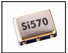
ANY-RATE I2C PROGRAMMABLE XO/VCXO

Features
Any-rate programmable outputfrequencies from 10 to 945 MHz andselect frequencies to 1.4 GHz
I2C serial interface
3rd generation DSPLL® with superiorjitter performance
3x better frequency stability thanSAW-based oscillators
Internal fixed crystal frequencyensures high reliability and lowaging
Available LVPECL, CMOS,LVDS, and CML outputs
Industry-standard 5x7 mmpackage
Pb-free/RoHS-compliant
1.8, 2.5, or 3.3 V supply
Applications
SONET / SDH
xDSL
10 GbE LAN / WAN
Low-jitter clock generation
Optical modules
Clock and data recovery
Description
The Si570 XO/Si571 VCXO utilizes Silicon Laboratories’ advanced DSPLL®circuitry to provide a low-jitter clock at any frequency. The Si570/Si571 areuser-programmable to any output frequency from 10 to 945 MHz and selectfrequencies to 1400 MHz with <1 ppb resolution. The device is programmedvia an I2C serial interface. Unlike traditional XO/VCXOs where a differentcrystal is required for each output frequency, the Si57x uses one fixedfrequencycrystal and a DSPLL clock synthesis IC to provide any-ratefrequency operation. This IC-based approach allows the crystal resonator toprovide exceptional frequency stability and reliability. In addition, DSPLLclock synthesis provides superior supply noise rejection, simplifying the taskof generating low-jitter clocks in noisy environments typically found incommunication systems.
Functional Block Diagram

· 吸波材料(NS1000),结构设计先进,可吸收泄露的电磁辐射,达到消除电磁干扰的目的,保证设备拥有好的屏蔽及EMI防护效果,经济环保,非常适合通信、仪器设备的使用。
责任编辑:Davia
【免责声明】
1、本文内容、数据、图表等来源于网络引用或其他公开资料,版权归属原作者、原发表出处。若版权所有方对本文的引用持有异议,请联系拍明芯城(marketing@iczoom.com),本方将及时处理。
2、本文的引用仅供读者交流学习使用,不涉及商业目的。
3、本文内容仅代表作者观点,拍明芯城不对内容的准确性、可靠性或完整性提供明示或暗示的保证。读者阅读本文后做出的决定或行为,是基于自主意愿和独立判断做出的,请读者明确相关结果。
4、如需转载本方拥有版权的文章,请联系拍明芯城(marketing@iczoom.com)注明“转载原因”。未经允许私自转载拍明芯城将保留追究其法律责任的权利。
拍明芯城拥有对此声明的最终解释权。


 产品分类
产品分类




 2012- 2022 拍明芯城ICZOOM.com 版权所有 客服热线:400-693-8369 (9:00-18:00)


