基于EFM8SB1/Si4460主控器件的管状电机微控制系统解决方案
 264
264
 拍明
拍明
概述
管状电机形如其名,是一种特殊的长条管状型的电机,广泛使用在遮阳系统,自动卷帘门窗,投影幕布等。管状电机一般采用无线遥控的控制方式,电机运行时容易干扰无线通信;而管状电机外壳是用金属制作,对无线信号造成屏蔽效应,造成通信距离变短。遥控器则采用电池供电,甚至有些管状电机也采用蓄电池或者锂电池供电。本方案中的无线收发器搭配超低功耗的MCU可实现低功耗远距离的目标,最大限度延长电池使用寿命。
优势
• 具备高性能超低功耗的8位MCU EFM8SB1( 88uA/MHz 运行功耗, 0.5uA 睡眠功耗),延长电池使用寿命,且3mm x 3mm QFN20 封装可满足遥控器或控制器小体积设计要求;
【EFM8SB1】
EFM8 Sleepy Bee Family EFM8SB1 Data Sheet
The EFM8SB1, part of the Sleepy Bee family of MCUs, is the world’s most energy friendly 8-bit microcontrollers with a comprehensive feature set in small packages.
These devices offer lowest power consumption by combining innovative low energy techniques and short wakeup times from energy saving modes into small packages, making them well-suited for any battery operated applications. With an efficient 8051 core, 14 high-quality capacitive sense channels, and precision analog, the EFM8SB1 family is also optimal for embedded applications.
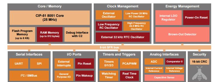
EFM8SB1 applications include the following:
• Touch pads / key pads
• Wearables
• Instrumentation panels
• Battery-operated consumer electronics
ENERGY FRIENDLY FEATURES
• Lowest MCU sleep current with supplybrownout (50 nA)
• Lowest MCU active current (150 μA / MHzat 24.5 MHz)
• Lowest MCU wake on touch averagecurrent (< 1 μA)
• Lowest sleep current using internal RTCand supply brownout (< 300 nA)
• Ultra-fast wake up for digital and analogperipherals (< 2 μs)
• Integrated LDO to maintain ultra-lowactive current at all voltages
Feature List
The EFM8SB1 highlighted features are listed below.
• Core:
• Pipelined CIP-51 Core
• Fully compatible with standard 8051 instruction set
• 70% of instructions execute in 1-2 clock cycles
• 25 MHz maximum operating frequency
• Memory:
• Up to 8 kB flash memory, in-system re-programmable from firmware.
• Up to 512 bytes RAM (including 256 bytes standard 8051 RAM and 256 bytes on-chip XRAM)
• Power:
• Internal LDO regulator for CPU core voltage
• Power-on reset circuit and brownout detectors
• I/O: Up to 17 total multifunction I/O pins:
• Flexible peripheral crossbar for peripheral routing
• 5 mA source, 12.5 mA sink allows direct drive of LEDs
• Clock Sources:
• Internal 20 MHz low power oscillator with ±10% accuracy
• Internal 24.5 MHz precision oscillator with ±2% accuracy
• Internal 16.4 kHz low-frequency oscillator or RTC 32 kHz crystal (RTC crystal not available on CSP16 packages)
• External crystal, RC, C, and CMOS clock options
• Timers/Counters and PWM:
• 32-bit Real Time Clock (RTC)
• 3-channel Programmable Counter Array (PCA) supporting PWM, capture/compare, and frequency output modes with watchdog timer function
• 4 x 16-bit general-purpose timers
• Communications and Digital Peripherals:
• UART
• SPI™ Master / Slave
• SMBus™ / I2C™ Master / Slave
• 16-bit CRC unit, supporting automatic CRC of flash at 256-byte boundaries
• Analog:
• Capacitive Sense (CS0)
• Programmable current reference (IREF0)
• 12-Bit Analog-to-Digital Converter (ADC0)
• 1 x Low-current analog comparator
• On-Chip, Non-Intrusive Debugging
• Full memory and register inspection
• Four hardware breakpoints, single-stepping
• Pre-loaded UART bootloader
• Temperature range -40 to 85 ºC
• Single power supply 1.8 to 3.6 V
• QSOP24, QFN24, QFN20, and CSP16 packages
With on-chip power-on reset, voltage supply monitor, watchdog timer, and
clock oscillator, the EFM8SB1 devices are truly standalone system-on-a-chip
solutions. The flash memory is reprogrammable in-circuit, providing non-volatile
data storage and allowing field upgrades of the firmware. The on-chip debugging
interface (C2) allows non-intrusive (uses no on-chip resources), full speed,
in-circuit debugging using the production MCU installed in the final
application. This debug logic supports inspection and modification of memory and
registers, setting breakpoints, single stepping, and run and halt commands. All
analog and digital peripherals are fully functional while debugging. Each device
is specified for 1.8 to 3.6 V operation. Devices are AEC-Q100 qualified (Grade
3) and are available in 16- pin CSP, 20-pin QFN, 24-pin QFN, or 24-pin QSOP
packages. All package options are lead-free and RoHS compliant. Note: CSP
devices can be handled and soldered using industry standard surface mount
assembly techniques. However, because CSP devices are essentially a piece of
silicon and are not encapsulated in plastic, they are susceptible to mechanical
damage and may be sensitive to light. When CSP packages must be used in an
environment exposed to light, it may be necessary to cover the top and sides
with an opaque material.
• 具备远距离高性能无线射频收发器Si4460,-129dbm 的超高接收灵敏度,10dbm 发射功率下传输距离大于1 千米,抗干扰性和穿墙性能好;10dbm 发射功率下工作电流18mA,接收电流约3mA(PSM 功能开启),睡眠功耗仅需740nA,适用电池供电的产品设计。
【Si4460】
Silicon Labs 的 EZRadioPRO 设备是高性能的低电流收发器,其覆盖了 119–1050 MHz 的 Sub-GHz 频段。这些收音机是 EZRadioPRO 系列的一部分,该系列包含覆盖各种应用的完整发射器、接收器和收发器产品线。EZRadioPRO 具有高达 -133 dBm 的出色灵敏度,同时实现极低的工作和待机电流消耗。此设备通过其集成片上 PA 展现出高达 +20 dBm 的卓越输出功率(活动模式 TX 电流消耗)。还包括唤醒定时器、低电量探测器,发射和接收数据 FIFO、上电复位电路和通用数字 I/O 等内置功能。
特点
IEEE 802.15.4g
无线 M-Bus
125 C° 的高温支持 (Si4468/7)
频率范围=119–1050 MHz
接收灵敏度 = -124 至 –133 dBm
调制
(G)FSK、(G)MSK、2(G)FSK、4(G)FSK
OOK
高达 +20 dBm 的最大输出功率
+27 dBm 或 +30 dBm 的 PA 支持
低活动功耗
前导码探测模式
10/13 mA RX
18 mA TX , +10 dBm (Si4460)
超低电流断电模式
30nA 关机,40 nA 待机
数据速率 =0.1 kbps 到 1 Mbps
电源 = 1.8 - 3.8 V
出色的选择性能
58 至 69 dB 相邻频道
1 MHz 处,阻断增益 > 73 dB
针对 >8 MHz 的偏移,阻断增益 > 84 dB
天线分集和 T/R 开关控制
高度可配置的分组处理程序
低 BOM
低电量探测器
Si4460/61/63/64/67/68 RF ICs Layout Design Guide
1. Introduction
The purpose of this application note is to help users design PCBs for the next generation EZRadioPRO™ RF ICs,i.e. the Si4460/61/63/64/67/68 devices (henceforth referred to as EZRadioPRO™ RF ICs) using good designpractices that allow for good RF performance. The matching principles described in detail in “AN627: Si4460/61/67
Low-Power PA Matching” and in “AN648: Si4063/Si4463/64/68 TX Matching”.
The RF performance and the critical maximum peak voltage on the output pin strongly depend on the PCB layoutas well as the design of the matching networks. For optimal performance, Silicon Labs recommends the use of thePCB layout design hints described in the following sections.
2. Design Recommendations when Using Si4460/61/63/64/67/68 RF ICs
》Extensive testing has been completed using reference designs provided by Silicon Labs. It isrecommended that designers use the reference designs “as-is” since theyminimizedetuning effectscaused by parasitics or generated by poor component placement and PCB routing.
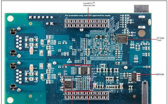
》The compact RF part of the designs is highlighted by a silkscreen frame, and it is strongly recommended touse the same framed RF layout in order to avoid any possibility of detuning effects. Figure 1 shows theframed compact RF part of the designs.
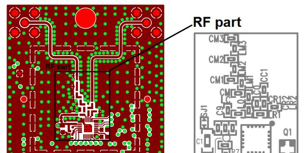
Figure 1. Compact RF Part of the Designs Highlighted on Top Silkscreen
》When layouts cannot be followed as shown by the reference designs (due to PCB size and shapelimitations), the layout design rules described in the following sections are recommended.
The Si4460/61/63/64/67/68 devices can use the following TX matching networks:
》Class E (CLE)
》Switched Current (SWC)
》Square-Wave (SQW)
The basic types of board layout configurations are as follows:
》Split TX/RX
》Direct Tie
》Switched TX/RX
》Diversity
In the Split TX/RX type, the TX and RX paths are separated, and individual SMA connectors are provided for each
path. This type of Pico Board is best suited to demonstrations of the output power and sensitivity of the
EZRadioPRO™ RF ICs.
In the Direct Tie type, the TX and RX paths are connected together directly, without any additional RF switch.
In the Switched TX/RX type, the boards contain a single antenna and a single-pole double-throw (SPDT) RF switch
to select between the TX and RX paths.
In the Diversity type, there are two antennas, both of which can be connected either to the TX or the RX path by a double-pole double-throw (DPDT) RF switch.
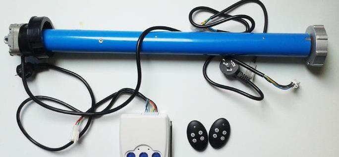
管状电机是一种高性能管状电机,包括管状机壳以及通过轴承座支撑在管状机壳内的驱动总成、刹车总成和行程控制总成,其刹车总成包括电机右轴固定件、右轴、电磁铁右轴固定件、电磁铁、栱杆制动机构;电机右轴固定件固定在低速电机的右端面,用以支撑右轴的一端;电磁铁右轴固定件安装在右轴上,电磁铁固定在电磁铁右轴固定件上,栱杆制动机构安装在右轴上并位于右轴与管状机壳之间的空腔内,电磁铁驱动栱杆制动机构进行制动。管状电机也具有占用面积小的特点。
责任编辑:Davia
【免责声明】
1、本文内容、数据、图表等来源于网络引用或其他公开资料,版权归属原作者、原发表出处。若版权所有方对本文的引用持有异议,请联系拍明芯城(marketing@iczoom.com),本方将及时处理。
2、本文的引用仅供读者交流学习使用,不涉及商业目的。
3、本文内容仅代表作者观点,拍明芯城不对内容的准确性、可靠性或完整性提供明示或暗示的保证。读者阅读本文后做出的决定或行为,是基于自主意愿和独立判断做出的,请读者明确相关结果。
4、如需转载本方拥有版权的文章,请联系拍明芯城(marketing@iczoom.com)注明“转载原因”。未经允许私自转载拍明芯城将保留追究其法律责任的权利。
拍明芯城拥有对此声明的最终解释权。


 产品分类
产品分类




 2012- 2022 拍明芯城ICZOOM.com 版权所有 客服热线:400-693-8369 (9:00-18:00)


