ADI ADUM4221 4A隔离的半桥栅极驱动器解决方案
 141
141
 拍明
拍明
原标题:ADI ADUM4221 4A隔离的半桥栅极驱动器解决方案
ADI公司的ADUM4221是4A输出隔离的半桥栅极驱动器,采用了该公司的iCoupler®技术,提供独立和隔离的高边和低边输出.它的隔离电压为5700V rms.器件组合了高速CMOS和单片变压器技术,这些隔离元件提供了比通常的脉冲变压器和栅极驱动器组合体更加优异的性能特性. ADuM4221的逻辑输入电压从2.5V到6.5V,和低压系统兼容.和采用高压绝缘方法的栅极驱动器相比, ADuM4221具有输入和输出间真正的电流隔离的优势.器件内置了重叠保护,允许死区时间可调整.死区时间引脚(DT)和GDN1引脚间的单个电阻设定了高边输出和低边输出间的次级边的死区时间. ADuM4221的峰值电流为4A(<2 Ω RDSON_x).最大传输时延为44ns,高共模瞬态免疫力为150 kV/μs, 默认低输出, 5700Vrms持续1分钟,UL认证per UL 1577.结温工作温度125C.主要应用在开关电源,隔离IGBT/MOSFET栅极驱动器,工业逆变器和氮化镓(GaN)/碳化硅(SiC)兼容器件.本文介绍了ADUM4221自举半桥应用电路,评估板EVAL-ADuM4221EBZ主要特性,电路图,材料清单和PCB设计图.
The ADuM4221 is a 4 A isolated, half bridge gate driver that employs the Analog Devices, Inc., iCoupler® technology to provide independent and isolated high-side and low-side outputs. The ADuM4221 provides 5700 V rms isolation in the increased creepage wide body, 16-lead SOIC_IC package. Combining high speed CMOS and monolithic transformer technology, these isolation components provide outstanding performance characteristics superior to the alternatives, such as the combination of pulse transformers and gate drivers.
The isolators operate with a logic input voltage ranging from 2.5 V to 6.5 V, providing compatibility with lower voltage systems. In comparison to gate drivers employing high voltage level translation methodologies, the ADuM4221 offers the benefit of true, galvanic isolation between the input and each output.
The ADuM4221 has a built in overlap protection and allows for dead time adjustment. A single resistor between the dead time pin (DT) and the GND1 pin sets the dead time on the secondary side between the high-side and the low-side outputs.
An internal thermal shutdown (TSD) sets outputs low if the internal temperature on the ADuM4221 exceeds the TSD temperature. As a result, the ADuM4221 provides reliable control over the switching characteristics of the insulated gate bipolar transistor (IGBT)/metal-oxide semiconductor field effect transistor (MOSFET) configurations over a wide range of positive or negative switching voltages.
ADUM4221主要特性:
4 A peak current (<2 Ω RDSON_x)
2.5 V to 6.5 V logic input voltage
4.5 V to 35 V output supply voltage
UVLO VDD1 positive going threshold: 2.5 V maximum
Multiple UVLO options for VDDA and VDDB positive going threshold
Grade A: 4.5 V maximum
Grade B: 7.5 V maximum
Grade C: 11.6 V maximum
Precise timing characteristics
44 ns maximum propagation delay
Adjustable dead time
CMOS input logic levels
High common-mode transient immunity: 150 kV/μs
High junction temperature operation: 125C
Default low output
Safety and regulatory approvals (pending)
UL recognition per UL 1577
5700 V rms for 1 minute duration
CSA Component Acceptance Notice 5A (pending)
VDE certificate of conformity (pending)
DIN V VDE V 0884-11
VIORM = 849 V peak
Increased creepage wide body, 16-lead SOIC_IC
ADUM4221应用:
Switching power supplies
Isolated IGBT/MOSFET gate drives
Industrial inverters
Gallium nitride (GaN)/silicon carbide (SiC) compatible

图1. ADUM4221自举半桥应用电路
评估板EVAL-ADuM4221EBZ
The EVAL-ADuM4221EBZ supports the ADuM4221 half bridge gate driver that employs Analog Devices, Inc., iCoupler® technology to provide independent and isolated high-side and low-side outputs. The EVAL-ADuM4221EBZ is populated with the ADuM4221, which has VIA and VIB inputs and dead time control. The EVAL-ADuM4221EBZ supplies jumpers and screw terminals to configure different drive conditions. The EVAL-ADuM4221EBZ operates with square waves and dc values on the VIA, VIB, and DISABLE pins.
The ADuM4221 operates with an input supply ranging from 2.5 V to 6.5 V, providing compatibility with lower voltage systems. Logic level voltages at the input pins control the VOA and VOB outputs. The driver has a DISABLE input pin that, if held high, shuts the device off regardless of the input on the channels. In addition to basic overlap protection, the dead time (DT) pin on the primary side allows an adjustable dead time between the VOA and VOB output transitions.
The ADuM4221 provides operation with voltages of up to 35 V on the secondary side. The EVAL-ADuM4221EBZ has a provision for the high-side supply to be bootstrapped to the low-side supply. The EVAL-ADuM4221EBZ facilitates testing of the propagation delay, drive strength, dead time operation, and input logic of the device. Because the EVAL-ADuM4221EBZ has footprints for insulated gate bipolar transistors (IGBTs) and metal-oxide semiconductor field effect transistors (MOSFETs) in TO-220 and TO-252 packages, the ADuM4221 can be evaluated with many different power devices.
For complete information about the ADuM4221, refer to the ADuM4221 data sheet in conjunction with this user guide when using the EVAL-ADuM4221EBZ.
评估板EVAL-ADuM4221EBZ主要特性:
Adjustable dead time
Output voltage range to 35 V
Screw terminals for easy connectivity
Pad placement for external series gate resistors
Pad placement for capacitive load testing
Supports TO-220 or TO-252 IGBTs or MOSFETs
Bootstrap option
Jumper placement for easy half bridge setup
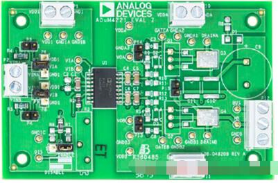
图2. 评估板EVAL-ADuM4221EBZ外形图
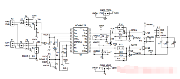
图3. 评估板EVAL-ADuM4221EBZ电路图
责任编辑:David
【免责声明】
1、本文内容、数据、图表等来源于网络引用或其他公开资料,版权归属原作者、原发表出处。若版权所有方对本文的引用持有异议,请联系拍明芯城(marketing@iczoom.com),本方将及时处理。
2、本文的引用仅供读者交流学习使用,不涉及商业目的。
3、本文内容仅代表作者观点,拍明芯城不对内容的准确性、可靠性或完整性提供明示或暗示的保证。读者阅读本文后做出的决定或行为,是基于自主意愿和独立判断做出的,请读者明确相关结果。
4、如需转载本方拥有版权的文章,请联系拍明芯城(marketing@iczoom.com)注明“转载原因”。未经允许私自转载拍明芯城将保留追究其法律责任的权利。
拍明芯城拥有对此声明的最终解释权。


 产品分类
产品分类




 2012- 2022 拍明芯城ICZOOM.com 版权所有 客服热线:400-693-8369 (9:00-18:00)


