


 产品分类
产品分类
Avago MGA-231T6 GPS低噪音(LNA)放大方案
 102
102
 拍明
拍明
原标题:Avago MGA-231T6 GPS低噪音(LNA)放大方案
Avago 公司的MGA-231T6 是(0.9-3.5)GHz GPS//ISM/WIMAX低噪音放大器(LNA),采用GaAs 增强模式pHEMT工艺,具有高增益.低噪音和高线性特性,工作定压可低至1.8V,主要用作GPS, WLAN 和WIMAX低噪音放大器.本文介绍了MGA-231T6主要特性, 演示板,应用电路和所用元件表以及S参数测量参考平面.
Avago Technologies’ MGA-231T6 is a low-noise amplifier (LNA) designed for GPS/ISM/Wimax applications in the (0.9-3.5)GHz frequency range. The LNA uses Avago Technologies’ proprietary GaAs Enhancement-mode pHEMT process to achieve high gain with very low noise figure and high linearity. Noise figure distribution is very tightly controlled. A CMOS-compatible shutdown pin is included either for turning the LNA on/off or for current adjustment.
The low noise figure and high gain, coupled with low current consumption make it suitable for use in critical low-power GPS applications or during low-battery situations.
MGA-231T6主要特性:
• Very Low Noise Figure
• High Gain and Linearity
• Low External Component Count
• Low Shutdown Current
• CMOS compatible shutdown pin (SD) current @ Vsd= 1.8V : 0.11mA
• Useable down to 1.8V supply
• Adjustable current via single external resistor/voltage
• Small package dimension: 2.0(L)x1.3(W)x0.4(H) mm Specifications (Typical performance @ 25°C) At 1.575GHz
• Vdd = 2.85V, Vsd = 1.8V, Idd =4mA
– Gain = 17.1 dB
– NF = 1.06 dB
– Input IP3 = 0.2 dBm
– Input P1dB = 7.7 dBm
MGA-231T6应用:
• LNA for GPS, WLAN and WIMAX

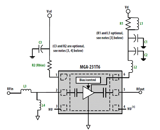
图1.MGA-231T6演示板和应用电路元件表
Notes:
1. Pin 4 must be left unconnected
2. L3 and L4 form the input matching network. C2 and L2 form a matching network at the output of the LNA.
3. L1 and R1 isolates the demoboard from external disturbances during measurement. It is not needed in actual application. Likewise, C1 and C3 mitigate the effect of external noise pickup on the Vdd and SD lines respectively. These components are not required in actual operation.
4. Bias control is achieved by either varying the SD voltage with/without R2, or fixing the SD voltage to Vdd and adjusting R2 for the desired current. R2 = 8.2 kOhm will result in 4mA when Vdd = 2.85V, Vsd = 1.8V or Vdd = 1.8V, Vsd = 2.6V. R2 = 5.6 kOhm will result in 6mA when Vdd = Vsd = 2.7V.
图2.MGA-231T6演示板和应用电路图
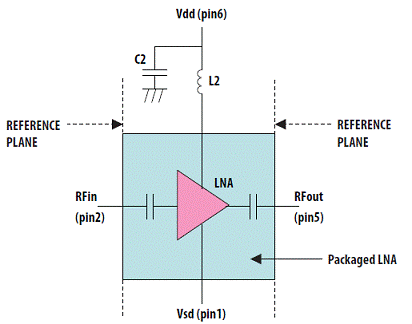
图3.MGA-231T6 S参数测量参考平面
责任编辑:David
【免责声明】
1、本文内容、数据、图表等来源于网络引用或其他公开资料,版权归属原作者、原发表出处。若版权所有方对本文的引用持有异议,请联系拍明芯城(marketing@iczoom.com),本方将及时处理。
2、本文的引用仅供读者交流学习使用,不涉及商业目的。
3、本文内容仅代表作者观点,拍明芯城不对内容的准确性、可靠性或完整性提供明示或暗示的保证。读者阅读本文后做出的决定或行为,是基于自主意愿和独立判断做出的,请读者明确相关结果。
4、如需转载本方拥有版权的文章,请联系拍明芯城(marketing@iczoom.com)注明“转载原因”。未经允许私自转载拍明芯城将保留追究其法律责任的权利。
拍明芯城拥有对此声明的最终解释权。
相关资讯
:
基于MC33771主控芯片的新能源锂电池管理系统解决方案

AMIC110 32位Sitara ARM MCU开发方案

基于AMIC110多协议可编程工业通信处理器的32位Sitara ARM MCU开发方案

基于展讯SC9820超低成本LTE芯片平台的儿童智能手表解决方案

基于TI公司的AM437x双照相机参考设计

基于MTK6580芯片的W2智能手表解决方案


 2012- 2022 拍明芯城ICZOOM.com 版权所有 客服热线:400-693-8369 (9:00-18:00)


