


 产品分类
产品分类
Si52258PCIe时钟发生器解决方案
 209
209
 拍明
拍明
原标题:ilabs Si52258PCIe时钟发生器解决方案
Silabs公司的Si52258/54是用于PCIe Gen1/2/3/4/5公共时钟和/或SRIS的业界最高性能和最低功耗汽车级的PCIe时钟发生器,所有时钟和PCIe Gen1/2/3/4/5公共时钟与单独基准架构指标兼容,硬件控制引脚可用来启动和禁止输出,以及启动和禁止扩展频谱用来降低EMI.Si52258/54具有内部终端的8/4输出,和PCIe Gen 1/2/3/4/5兼容,汽车级2工作温度–40 到 +105℃,内部100 Ω 或85 Ω电阻线路匹配,具有极好的抖动性能: Gen3/4为0.05 ps RMS, Gen5为0.025 ps RMS.三角扩展频谱用来降低EMI,可低至0.25%或0.5%,单独硬件控制引脚用来输出使能,扩展频谱使能,25MHz晶振输入或时钟输入,工作电压1.8V-3.3V,无铅RoHS-6兼容.主要用在信息娱乐设备, ADAS ECU,雷达传感器和激光雷达(LiDar)传感器.本文介绍了Si52258主要特性和特性列表,框图以及评估板Si52258-EVB主要特性,功能框图和主要特性,电路图,材料清单和PCB设计图.
The Si52258/54 are the industry’s highest performance and lowest power automotive grade PCI Express clock generators for PCIe Gen1/2/3/4/5 common clock and/or SRIS applications. The Si52258 and Si52254 source eight and four 100 MHz PCIe differential clock outputs, respectively. All clock outputs are compliant to PCIe Gen1/2/3/4/5 common clock and separate reference clock architecture specifications.
Hardware control pins are available for enabling and disabling the outputs, as well as spread spectrum enable/disable for EMI reduction.
For more information about PCI Express, Silicon Labs’ complete PCIe portfolio, applicationnotes, and design tools, including the Silicon Labs PCIe Clock Jitter Tool for PCI Expresscompliance, please visit the Silicon Labs PCI Express Learning Center.
Si52258主要特性:
• 8/4-outputs with internal termination
• PCIe Gen 1/2/3/4/5 compliant
• Automotive grade 2: –40 to +105℃
• Internal 100 Ω or 85 Ω line matching
• Excellent jitter performance
• 0.05 ps RMS (Gen3/4)
• 0.025 ps RMS (Gen5)
• Triangular spread spectrum for EMIreduction, down spread 0.25% or 0.5%
• Individual hardware control pins for OutputEnable, Spread Spectrum Enable
• Enable and Frequency Select
• 25 MHz crystal input or clock input
• 1.8–3.3 V power supply
• Pb-free, RoHS-6 compliant
Si52258应用:
• Infotainment
• ADAS ECU
• Radar Sensors
• LiDar Sensors
Si52258特性列表:
• 8/4-outputs with internal termination
• PCIe Gen1/2/3/4/5 compliant
• Automotive grade 2: –40 to +105℃
• Internal 100 Ω or 85 Ω line matching
• Excellent jitter performance
• 0.05 ps RMS (Gen3/4)
• 0.025 ps RMS (Gen5)
• Triangular spread spectrum for EMI reduction, down spread 0.25% or 0.5%
• Individual hardware control pins for Output Enable, Spread Spectrum Enable
• Enable and Frequency Select
• 25 MHz crystal input or clock input
• 1.8–3.3 V power supply
• Pb-free, RoHS-6 compliant
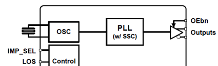
图1.Si5225x系列框图
评估板Si52258-EVB
The Si52258-EVB is used for evaluating the eight output Si52258A-D01AM Automotive gradePCIe Reference Clock Generator. The Si52258A-D01AM device uses the on-board 25 MHz crystal as reference clock source and generates 8 copies of a 100 MHz HCSL format output clock compliant to PCIe Gen 1/2/3/4/5 common clock and separate reference clock specifications.
评估板Si52258-EVB主要特性:
• Powered from either USB port or external +5Vpower supply.
• On-board 25 MHz crystal reference.
• Programmable device core VDD supply foroperation at 3.3 V, 2.5 V, or 1.8 V.
• Programmable VDDO (output driver) suppliesallow each of the clock output banks to have itsown power supply voltage selectable from 3.3V, 2.5 V, or 1.8 V.
• SMA connectors for all output clocks.
• PCIe compliant spread spectrum enabled/disabled via on-board switch.
• Internal output termination switch selectable for100 Ω or 85 Ω operation.
• Output enable (OE) control switch per output.
• All output trace lengths matched to 10 inches.
• Loss of Signal (LOS) indication LED.
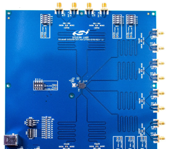
图2.评估板Si52258-EVB外形图
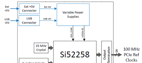
图3.评估板Si52258-EVB功能框图
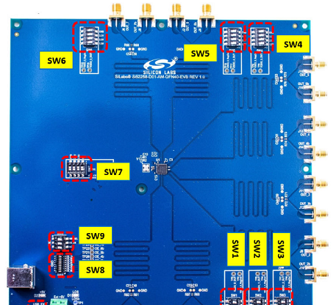
图4.评估板Si52258-EVB DIP开关位置图
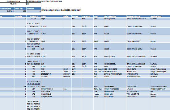
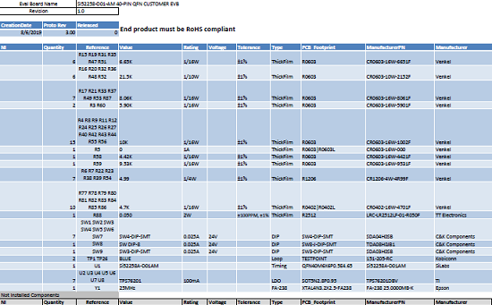
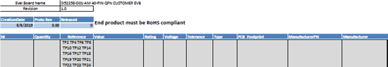
评估板Si52258-EVB材料清单:
责任编辑:David
【免责声明】
1、本文内容、数据、图表等来源于网络引用或其他公开资料,版权归属原作者、原发表出处。若版权所有方对本文的引用持有异议,请联系拍明芯城(marketing@iczoom.com),本方将及时处理。
2、本文的引用仅供读者交流学习使用,不涉及商业目的。
3、本文内容仅代表作者观点,拍明芯城不对内容的准确性、可靠性或完整性提供明示或暗示的保证。读者阅读本文后做出的决定或行为,是基于自主意愿和独立判断做出的,请读者明确相关结果。
4、如需转载本方拥有版权的文章,请联系拍明芯城(marketing@iczoom.com)注明“转载原因”。未经允许私自转载拍明芯城将保留追究其法律责任的权利。
拍明芯城拥有对此声明的最终解释权。
相关资讯
:
基于MC33771主控芯片的新能源锂电池管理系统解决方案

AMIC110 32位Sitara ARM MCU开发方案

基于AMIC110多协议可编程工业通信处理器的32位Sitara ARM MCU开发方案

基于展讯SC9820超低成本LTE芯片平台的儿童智能手表解决方案

基于TI公司的AM437x双照相机参考设计

基于MTK6580芯片的W2智能手表解决方案


 2012- 2022 拍明芯城ICZOOM.com 版权所有 客服热线:400-693-8369 (9:00-18:00)


