


 产品分类
产品分类
ADI ADHV4702-124V至220V精密运算放大器解决方案
 87
87
 拍明
拍明
原标题:ADI ADHV4702-124V至220V精密运算放大器解决方案
ADI公司的ADHV4702-1是高压(220V)一增益稳定精密运算放大器,具有高输入阻抗和低输入偏压电流,低输入失调电压,低漂移和低噪音,对称工作电压±110 V,不对称单源工作电压220V,开环增益(AOL)170dB,共模抑制比(CMRR)160dB,最大事端失调电压(VOS) 2 μV/℃,输入噪音8 nV/√Hz ,主要用在高边电流检测,自动测试设备,高压驱动器,压电传感器以及数模转换器(DAC)输出缓冲器.本文介绍了ADHV4702-1主要特性,功能框图以及评估板EVAL-ADHV4702-1CPZ主要特性,电路图和材料清单.
The ADHV4702-1 is a high voltage (220 V), unity-gain stable precision operational amplifier. The ADHV4702-1 offers high input impedance with low input bias current, low input offset voltage, low drift, and low noise for precision demanding applications. The next generation of proprietary semiconductor processes and innovative architecture from Analog Devices, Inc., enable this precision operational amplifier to operate from symmetrical dual supplies of ±110 V, asymmetrical dual supplies, or a single supply of 220 V.
For precision performance, the ADHV4702-1 has a 170 dB typical open-loop gain (AOL) and a 160 dB typical common-mode rejection ratio (CMRR), as shown in Figure 2. The ADHV4702-1 also has a 2 μV/℃ maximum input offset voltage (VOS) drift and an 8 nV/√Hz input voltage noise.
The exceptional dc precision of the ADHV4702-1 is complemented by excellent dynamic performance with a small signal bandwidth of 10 MHz and a slew rate of 74 V/μs. The ADHV4702-1 has an output current of 20 mA typical.
The ADHV4702-1 offers high voltage input common-mode swing as well as high voltage output swing, enabling precision high voltage use cases such as high-side current sensing. The ADHV4702-1 is also ideally suited for forcing a voltage in precision bias and control applications.
The ADHV4702-1 is available in a 12-lead, 7 mm × 7 mm lead frame chip scale package (LFCSP) with an exposed pad (EPAD) compliant to international electrotechnical commission (IEC) 61010-1 creepage and clearance standards. The copper EPAD provides a low thermal resistance path to improve heat dissipation and features high voltage isolation, allowing it to be safely connected to a 0 V ground plane regardless of VCC or VEE voltages. The ADHV4702-1 operates over the −40℃ to +85℃ industrial temperature range.
ADHV4702-1主要特性:
Wide range of operating voltages
Dual-supply: ±12 V to ±110 V
Asymmetrical supply operation: 24 V to 220 V
Wide input common-mode voltage range: 3 V from rails
High common-mode rejection ratio: 160 dB typical
High AOL: 170 dB typical
High slew rate
74 V/μs typical
24 V/μs typical with external input clamping diodes
Low input bias current: 2 pA maximum
Low input offset voltage: 1 mV maximum
Low input offset voltage drift: 2 μV/℃ maximum
Low input voltage noise: 8 nV/√Hz typical at 10 kHz
Wide small signal bandwidth: 10 MHz typical
Resistor adjustable quiescent current: 0.6 mA to 3 mA (VS = ±110 V)
Unity-gain stable
Thermal monitoring
Small footprint: 12-lead, 7 mm × 7 mm LFCSP compliant with IEC 61010-1 spacing
Shutdown mode
ADHV4702-1应用:
High-side current sensing
Automated test equipment
High voltage drivers
Piezotransducers
Digital-to-analog converter (DAC) output buffers
Light detecting and ranging (LiDAR), avalanche photodiode (APD), single photon avalanche diode (SPAD) biasing
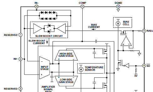
图1.ADHV4702-1功能框图
评估板EVAL-ADHV4702-1CPZ
This user guide describes the EVAL-ADHV4702-1CPZ evalua-tion board, which helps users evaluate the ADHV4702-1 offered in a 7 mm × 7 mm, 12-lead lead frame chip scale package (LFCSP) with an exposed pad at the bottom. The evaluation board provides a platform for quick and easy evaluation of the ADHV4702-1. Figure 1 shows the top side of the evaluation board. Figure 2 shows the bottom side of the board with the large exposed copper area for attaching a heat sink to provide additional thermal management.
The evaluation board is a 6-layer board designed to minimize leakage currents with its guard ring feature. It accepts Subminia-ture Version A (SMA) and Subminiature Version B (SMB) edge mounted connectors on the inputs for easy connection to test equipment or other circuitry.
The ADHV4702-1 data sheet covers the specifications and details of the device operation and application circuit configurations and guidance. Full specifications of the ADHV4702-1 can be found in the ADHV4702-1 data sheet, available from Analog Devices, Inc., and must be consulted in conjunction with this user guide, especially when powering up the evaluation board for the first time.
For safety, the EVAL-ADHV4702-1CPZ evaluation board is covered top and bottom with acrylic plastic guards to reduce the risk of inadvertent contact with high voltage. Do not operate the board without these guards in place. If the guards must be removed to adjust jumpers or change component values, discon-nect the board from the power supply before removing guards, and replace the guards before powering up again. For full precautions when using this high voltage evaluation board, see the High Voltage Evaluation Board section.
评估板EVAL-ADHV4702-1CPZ主要特性:
Full featured evaluation board for the ADHV4702-1
Single-supply or dual-supply operation
On-board power management circuit generates high voltage
Edge mounted SMA and SMB connector provisions
Easy connection to test equipment and other circuits
Robust thermal management
评估板EVAL-ADHV4702-1CPZ包括:
EVAL-ADHV4702-1CPZ evaluation board
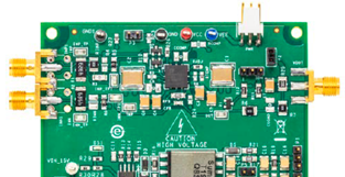
图2.评估板EVAL-ADHV4702-1CPZ外形图(正面)

图3.评估板EVAL-ADHV4702-1CPZ外形图(背面)
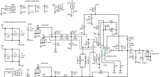
图4.评估板EVAL-ADHV4702-1CPZ电路图(1)
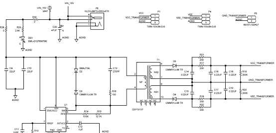
图5.评估板EVAL-ADHV4702-1CPZ电路图(2)
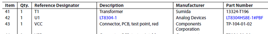
评估板EVAL-ADHV4702-1CPZ材料清单:

责任编辑:David
【免责声明】
1、本文内容、数据、图表等来源于网络引用或其他公开资料,版权归属原作者、原发表出处。若版权所有方对本文的引用持有异议,请联系拍明芯城(marketing@iczoom.com),本方将及时处理。
2、本文的引用仅供读者交流学习使用,不涉及商业目的。
3、本文内容仅代表作者观点,拍明芯城不对内容的准确性、可靠性或完整性提供明示或暗示的保证。读者阅读本文后做出的决定或行为,是基于自主意愿和独立判断做出的,请读者明确相关结果。
4、如需转载本方拥有版权的文章,请联系拍明芯城(marketing@iczoom.com)注明“转载原因”。未经允许私自转载拍明芯城将保留追究其法律责任的权利。
拍明芯城拥有对此声明的最终解释权。
相关资讯
:
基于MC33771主控芯片的新能源锂电池管理系统解决方案

AMIC110 32位Sitara ARM MCU开发方案

基于AMIC110多协议可编程工业通信处理器的32位Sitara ARM MCU开发方案

基于展讯SC9820超低成本LTE芯片平台的儿童智能手表解决方案

基于TI公司的AM437x双照相机参考设计

基于MTK6580芯片的W2智能手表解决方案


 2012- 2022 拍明芯城ICZOOM.com 版权所有 客服热线:400-693-8369 (9:00-18:00)


