


 产品分类
产品分类
Lattice ECP3 FPGA系列AMC评估开发方案
 67
67
 拍明
拍明
原标题:Lattice ECP3 FPGA系列AMC评估开发方案
lattice公司的LatticeECP3 FPGA系列可提供高性能特性如增强的DSP架构,高速SERDES和高速源同步接口. LatticeECP3采用65nm技术,查找表(LUT)高达149K逻辑单元,支持高达486个用户I/O,提供高达320个18x18乘法器和各种并行I/O标准,主要用于对成本和功耗敏感的无线基础设备和有线通信.本文介绍了LatticeECP3 FPGA主要特性和方框图,以及Lattice ECP3 AMC评估板和接口板的主要特性,电路图以及材料清单(BOM).
The LatticeECP3™ (EConomy Plus Third generation) family of FPGA devices is optimized to deliver high performance features such as an enhanced DSP architecture, high speed SERDES and high speed source synchronous interfaces in an economical FPGA fabric. This combination is achieved through advances in device architecture and the use of 65nm technology making the devices suitable for high-volume, high-speed, low-cost applications. The LatticeECP3 device family expands look-up-table (LUT) capacity to 149K logic elements and supports up to 486 user I/Os. The LatticeECP3 device family also offers up to 320 18x18 multipliers and a wide range of parallel I/O standards. The LatticeECP3 FPGA fabric is optimized with high performance and low cost in mind. The LatticeECP3 devices utilize reconfigurable SRAM logic technology and provide popular building blocks such as LUT-based logic, distrib-uted and embedded memory, Phase Locked Loops (PLLs), Delay Locked Loops (DLLs), pre-engineered source synchronous I/O support, enhanced sysDSP slices and advanced configuration support, including encryption and dual-boot capabilities. The pre-engineered source synchronous logic implemented in the LatticeECP3 device family supports a broad range of interface standards, including DDR3, XGMII and 7:1 LVDS. The LatticeECP3 device family also features high speed SERDES with dedicated PCS functions. High jitter toler-ance and low transmit jitter allow the SERDES plus PCS blocks to be configured to support an array of popular data protocols including PCI Express, SMPTE, Ethernet (XAUI, GbE, and SGMII) and CPRI. Transmit Pre-empha-sis and Receive Equalization settings make the SERDES suitable for transmission and reception over various forms of media. The LatticeECP3 devices also provide flexible, reliable and secure configuration options, such as dual-boot capa-bility, bit-stream encryption, and TransFR field upgrade features. The ispLEVER® design tool suite from Lattice allows large complex designs to be efficiently implemented using the LatticeECP3 FPGA family. Synthesis library support for LatticeECP3 is available for popular logic synthesis tools. The ispLEVER tool uses the synthesis tool output along with the constraints from its floor planning tools to place and route the design in the LatticeECP3 device. The ispLEVER tool extracts the timing from the routing and back-annotates it into the design for timing verification. Lattice provides many pre-engineered IP (Intellectual Property) ispLeverCORE™ modules for the LatticeECP3 family. By using these configurable soft core IPs as standardized blocks, designers are free to concentrate on the unique aspects of their design, increasing their productivity.
LatticeECP3 FPGA主要特性:
Higher Logic Density for Increased System Integration
• 17K to 149K LUTs
• 133 to 586 I/Os
Embedded SERDES
• 150 Mbps to 3.2 Gbps for Generic 8b10b, 10-bit SERDES, and 8-bit SERDES modes
• Data Rates 230 Mbps to 3.2 Gbps per channel for all other protocols
• Up to 16 channels per device: PCI Express, SONET/SDH, Ethernet (1GbE, SGMII, XAUI), CPRI, SMPTE 3G and Serial RapidIO
sysDSP™
• Fully cascadable slice architecture
• 12 to 160 slices for high performance multiply and accumulate
• Powerful 54-bit ALU operations
• Time Division Multiplexing MAC Sharing
• Rounding and truncation
• Each slice supports
–Half 36x36, two 18x18 or four 9x9 multipliers
–Advanced 18x36 MAC and 18x18 Multiply-Multiply-Accumulate (MMAC) operations
Flexible Memory Resources
• Up to 6.85Mbits sysMEM™ Embedded Block RAM (EBR)
• 36K to 303K bits distributed RAM
sysCLOCK Analog PLLs and DLLs
• Two DLLs and up to ten PLLs per device
Pre-Engineered Source Synchronous I/O
• DDR registers in I/O cells
• Dedicated read/write levelling functionality
• Dedicated gearing logic
• Source synchronous standards support
–ADC/DAC, 7:1 LVDS, XGMII
–High Speed ADC/DAC devices
• Dedicated DDR/DDR2/DDR3 memory with DQS support
• Optional Inter-Symbol Interference (ISI) correction on outputs
Programmable sysI/O™ Buffer Supports Wide Range of Interfaces
• On-chip termination
• Optional equalization filter on inputs
• LVTTL and LVCMOS 33/25/18/15/12
• SSTL 33/25/18/15 I, II
• HSTL15 I and HSTL18 I, II
• PCI and Differential HSTL, SSTL
• LVDS, Bus-LVDS, LVPECL, RSDS, MLVDS
Flexible Device Configuration
• Dedicated bank for configuration I/Os
• SPI boot flash interface
• Dual-boot images supported
• Slave SPI
• TransFR™ I/O for simple field updates
• Soft Error Detect embedded macro
System Level Support
• IEEE 1149.1 and IEEE 1532 compliant
• Reveal Logic Analyzer
• ORCAstra FPGA configuration utility
• On-chip oscillator for initialization & general use
• 1.2V core power supply
LatticeECP3™系列性能表:
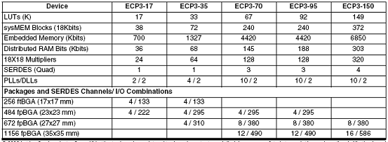
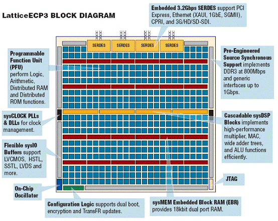
图1. LatticeECP3方框图
Lattice ECP3 AMC 评估板
The LatticeECP3™ Advanced Mezzanine Card (AMC) Evaluation Board allows designers to investigate and experiment with the features of the LatticeECP3 high-speed SERDES transceivers in an AMC system environment. The features of the LatticeECP3 AMC Evaluation Board assist engineers with rapid prototyping and testing of their designs. The board follows portions of the PICMG AMC R2.0 AMC form-factor specification that allows users the capability to use the board in live system evaluations. This user’s guide is intended to be referenced in conjunction with evaluation design tutorials to demonstrate the LatticeECP3 FPGA.
Lattice ECP3 AMC评估板主要特性:
• Single module AMC PCB card edge interface
–Allows demonstration of AMC Fat Pipes
–Common options interface
• Allows control of SERDES PCS registers using the Serial Client Interface (ORCAstra)
• DMC (FPGA Mezzanine Card) expansion connector
• USB-B connection to UART for run-time control
• RJ45 interface to 10/100/1000 Ethernet to SGMII
• SFP transceiver module cage and connection
• On-board Boot Flash
–64M Serial SPI Flash
• DDR2 memory components (256MB x 32 bits)
• 32-bit parallel, non-volatile memory that can be read, erased and reprogrammed
• Switches, LEDs and displays for demonstration purposes
• ispVM™ System software programming support
• On-board reference clock sources
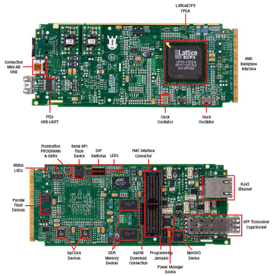
图2. Lattice ECP3 AMC评估板外形图
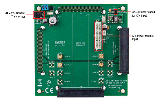
图3. Lattice ECP3 AMC接口板外形图
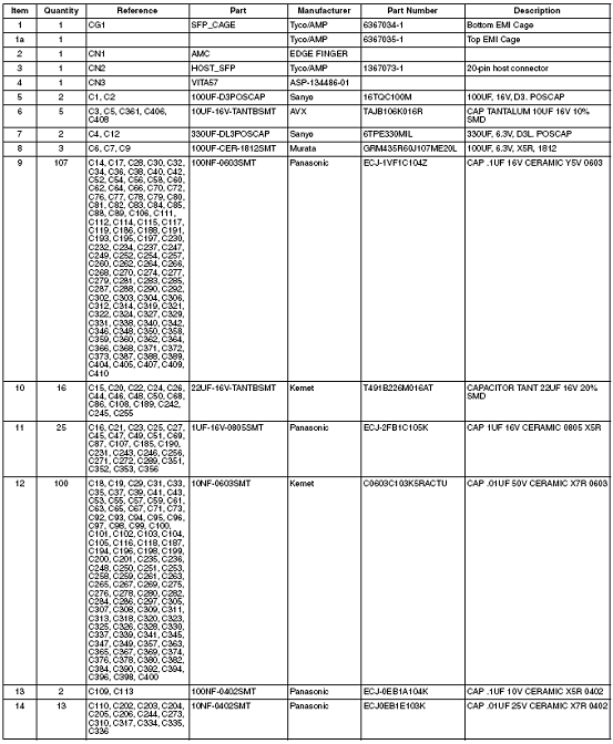
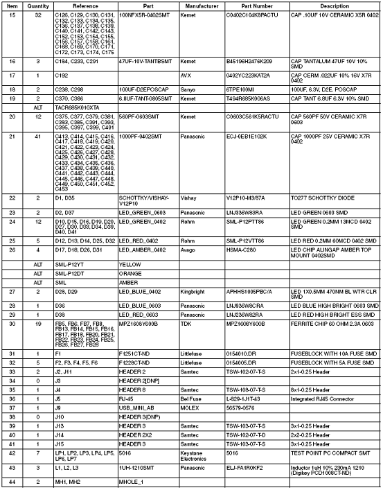
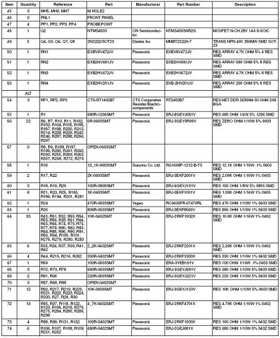
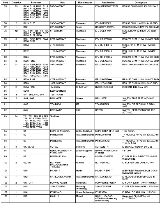
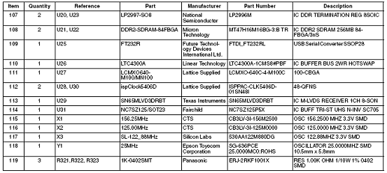
LatticeECP3 AMC评估板材料清单(BOM):
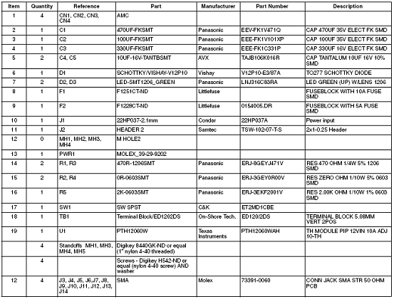
Lattice ECP3 AMC接口板材料清单(BOM):
责任编辑:HanFeng
【免责声明】
1、本文内容、数据、图表等来源于网络引用或其他公开资料,版权归属原作者、原发表出处。若版权所有方对本文的引用持有异议,请联系拍明芯城(marketing@iczoom.com),本方将及时处理。
2、本文的引用仅供读者交流学习使用,不涉及商业目的。
3、本文内容仅代表作者观点,拍明芯城不对内容的准确性、可靠性或完整性提供明示或暗示的保证。读者阅读本文后做出的决定或行为,是基于自主意愿和独立判断做出的,请读者明确相关结果。
4、如需转载本方拥有版权的文章,请联系拍明芯城(marketing@iczoom.com)注明“转载原因”。未经允许私自转载拍明芯城将保留追究其法律责任的权利。
拍明芯城拥有对此声明的最终解释权。
相关资讯
:
基于MC33771主控芯片的新能源锂电池管理系统解决方案

AMIC110 32位Sitara ARM MCU开发方案

基于AMIC110多协议可编程工业通信处理器的32位Sitara ARM MCU开发方案

基于展讯SC9820超低成本LTE芯片平台的儿童智能手表解决方案

基于TI公司的AM437x双照相机参考设计

基于MTK6580芯片的W2智能手表解决方案


 2012- 2022 拍明芯城ICZOOM.com 版权所有 客服热线:400-693-8369 (9:00-18:00)


