


 产品分类
产品分类
ST STM32F100VBT6 32位MCU开发评估方案
 108
108
 拍明
拍明
原标题:ST STM32F100VBT6 32位MCU开发评估方案
ST 公司的stm32F100VBT6采用ARM Cortex™-M3 32位RISC内核,工作频率24MHz,集成了高速嵌入式存储器(闪存高达128KB,SRAM高达8KB)以及各种增强外设和连接到两条APB总线的I/O.所有器件提供两个I2C,两个SPI,一个HDMI CEC和多达3个USART标致通信接口以及一个12位ADC,两个12位DAC和六个通用16位定时器和PWM定时器.主要用在控制和用户接口,医疗设备,PC和游戏机外设,GPS平台,工业应用,PLC,逆变器,打印机,视频通信和HVAC等.本文介绍了STM32F100VBT6主要特性, 方框图, 时钟树框图和电源框图以及STM32100B-EVAL评估板主要特性, 评估板硬件方框图和详细电路图.
STM32F100x4 STM32F100x6,STM32F100x8 STM32F100xB
Low & medium-density value line, advanced ARM-based 32-bit MCU with 16 to 128 KB Flash, 12 timers, ADC, DAC & 8 comm interfaces
The STM32F100xx value line family incorporates the high-performance ARM Cortex™-M3 32-bit RISC core operating at a 24 MHz frequency, high-speed embedded memories (Flash memory up to 128 Kbytes and SRAM up to 8 Kbytes), and an extensive range of enhanced peripherals and I/Os connected to two APB buses. All devices offer standard communication interfaces (up to two I2Cs, two SPIs, one HDMI CEC, and up to three USARTs), one 12-bit ADC, two 12-bit DACs, up to six general-purpose 16-bit timers and an advanced-control PWM timer.
The STM32F100xx low- and medium-density value line family operates in the –40 to +85 ℃ and –40 to +105℃ temperature ranges, from a 2.0 to 3.6 V power supply. A comprehensive set of power-saving mode allows the design of low-power applications.
The STM32F100xx value line family includes devices in three different packages ranging
from 48 pins to 100 pins. Depending on the device chosen, different sets of peripherals are included.
These features make the STM32F100xx value line microcontroller family suitable for a wide range of applications such as application control and user interfaces, medical and handheld equipment, PC and gaming peripherals, GPS platforms, industrial applications, PLCs, inverters, printers, scanners, alarm systems, video intercoms, and HVACs.
STM32F100VBT6主要特性:
■ Core: ARM 32-bit Cortex™-M3 CPU
– 24 MHz maximum frequency, 1.25 DMIPS/MHz (Dhrystone 2.1) performance
– Single-cycle multiplication and hardware division
■ Memories
– 16 to 128 Kbytes of Flash memory
– 4 to 8 Kbytes of SRAM
■ Clock, reset and supply management
– 2.0 to 3.6 V application supply and I/Os
– POR, PDR and programmable voltage detector (PVD)
– 4-to-24 MHz crystal oscillator
– Internal 8 MHz factory-trimmed RC
– Internal 40 kHz RC
– PLL for CPU clock
– 32 kHz oscillator for RTC with calibration
■ Low power
– Sleep, Stop and Standby modes
– VBAT supply for RTC and backup registers
■ Debug mode
– Serial wire debug (SWD) and JTAG interfaces
■ DMA
– 7-channel DMA controller
– Peripherals supported: timers, ADC, SPIs,
I2Cs, USARTs and DACs
■ 1 × 12-bit, 1.2 μs A/D converter (up to 16 channels)
– Conversion range: 0 to 3.6 V
– Temperature sensor
■ 2 × 12-bit D/A converters
■ Up to 80 fast I/O ports
– 37/51/80 I/Os, all mappable on 16 external interrupt vectors and almost all 5 V-tolerant
■ Up to 12 timers
– Up to three 16-bit timers, each with up to 4 IC/OC/PWM or pulse counter
– 16-bit, 6-channel advanced-control timer:
up to 6 channels for PWM output, dead time generation and emergency stop
– One 16-bit timer, with 2 IC/OC, 1 OCN/PWM, dead-time generation and emergency stop
– Two 16-bit timers, each with
IC/OC/OCN/PWM, dead-time generation and emergency stop
– 2 watchdog timers (Independent and Window)
– SysTick timer: 24-bit downcounter
– Two 16-bit basic timers to drive the DAC
■ Up to 8 communications interfaces
– Up to two I2C interfaces (SMBus/PMBus)
– Up to 3 USARTs (ISO 7816 interface, LIN, IrDA capability, modem control)
– Up to 2 SPIs (12 Mbit/s)
– Consumer electronics control (CEC) interface
■ CRC calculation unit, 96-bit unique ID
■ ECOPACK® packages
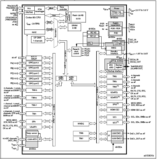
图1.STM32F100xx系列方框图
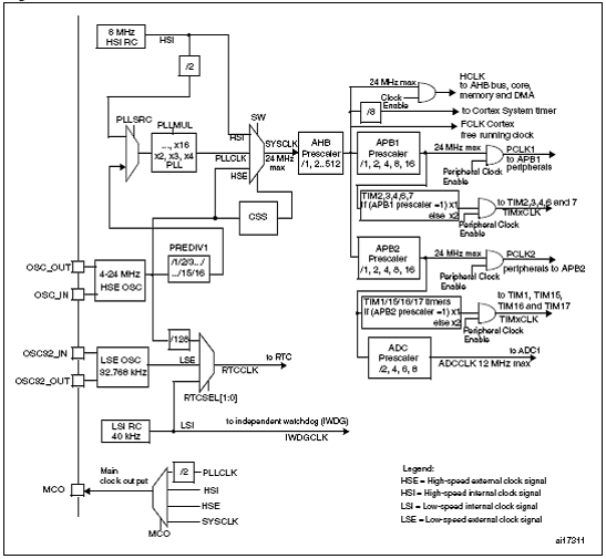
图2.STM32F100xx系列时钟树框图
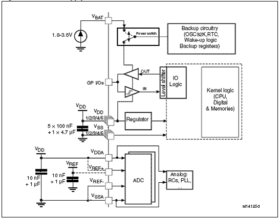
图3.STM32F100xx系列电源框图
STM32100B-EVAL评估板
The STM32100B-EVAL is an evaluation board for STMicroelectronic’s ARMTM Cortex-M3 core-based STM32F100VBT6 microcontroller. It is designed as a complete development environment with HDMI CEC, two I2C channels, two SPI channels, three USART channels, 8 KB internal SRAM and 128 KB internal Flash, and JTAG and SWD debugging support.
With a complete range of hardware evaluations features, the STM32100B-EVAL board is designed to help developers evaluate all device peripherals (such as HDMI CEC, motor control, LCD, MicroSD Card™, serial Flash, speaker, IrDA and USART) and develop their own applications. Extension connectors make it possible to easily connect a daughterboard or wrapping board for a specific application.
An ST-LINK is integrated on the board as an embedded in-circuit debugger and programmer for the STM32F100VBT6 MCU.
STM32100B-EVAL评估板主要特性:
● Three 5 V power supply options: power jack, ST-LINK connector or daughterboard
● Boot from user Flash, system memory or SRAM
● Speaker
● 1 Gbyte MicroSD Card™
● 16 Mbyte serial Flash
● I2C/SMBus compatible serial interface temperature sensor
● Two RS-232 communication channels with support for RTS/CTS handshake on one channel
● IrDA transceiver
● Induction motor control connector
● JTAG and SWD debug support
● 240x320 TFT color LCD
● Joystick with 4-direction control and selector
● Reset, wakeup, tamper and user push buttons
● Four LEDs
● RTC with backup battery
● Extension connector for daughterboard or wrapping board
● Embedded ST-LINK
● IDD current measurement circuit
● HDMI CEC
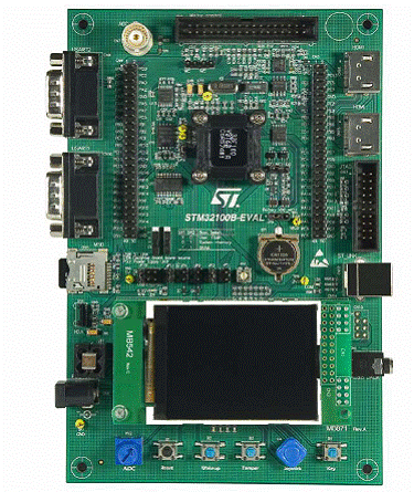
图4.STM32F100VBT6评估板(STM32100B-EVAL)外形图
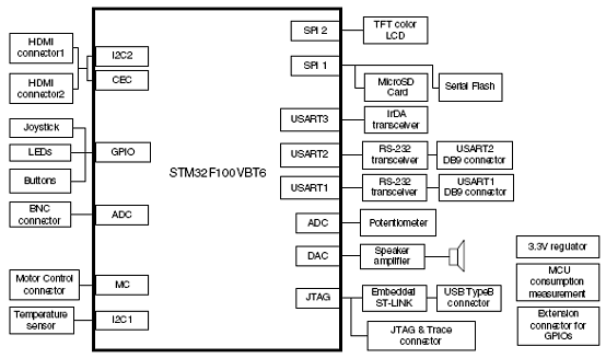
图5.STM32F100VBT6评估板硬件方框图
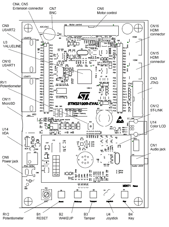
图5.STM32F100VBT6评估板布局图
责任编辑:HanFeng
【免责声明】
1、本文内容、数据、图表等来源于网络引用或其他公开资料,版权归属原作者、原发表出处。若版权所有方对本文的引用持有异议,请联系拍明芯城(marketing@iczoom.com),本方将及时处理。
2、本文的引用仅供读者交流学习使用,不涉及商业目的。
3、本文内容仅代表作者观点,拍明芯城不对内容的准确性、可靠性或完整性提供明示或暗示的保证。读者阅读本文后做出的决定或行为,是基于自主意愿和独立判断做出的,请读者明确相关结果。
4、如需转载本方拥有版权的文章,请联系拍明芯城(marketing@iczoom.com)注明“转载原因”。未经允许私自转载拍明芯城将保留追究其法律责任的权利。
拍明芯城拥有对此声明的最终解释权。
相关资讯
:
基于MC33771主控芯片的新能源锂电池管理系统解决方案

AMIC110 32位Sitara ARM MCU开发方案

基于AMIC110多协议可编程工业通信处理器的32位Sitara ARM MCU开发方案

基于展讯SC9820超低成本LTE芯片平台的儿童智能手表解决方案

基于TI公司的AM437x双照相机参考设计

基于MTK6580芯片的W2智能手表解决方案


 2012- 2022 拍明芯城ICZOOM.com 版权所有 客服热线:400-693-8369 (9:00-18:00)


