


 产品分类
产品分类
Freescale MC13260 SoC双向无线电解决方案
 61
61
 拍明
拍明
原标题:Freescale MC13260 SoC双向无线电解决方案
freescale公司的MC13260是系统级(SoC)双向无线电芯片,集成了32位ARM926EJ-S微控制器(工作速率高达150 MHz),高度优化的软件定义的矢量调制解调器处理器(工作速率高达100 MHz)和近1GHz RF收发器(60 MHz–960 MHz)以及混合信号模拟电路,支持语音和多种外设.主要用在完整的模拟FM无线电,数字无线电(DMR, dPMR, P25, Tetra等),双模式模拟FM和数字语音/数据以及蜂窝应用的”网络通话”.本文介绍了MC13260主要特性, MC13260各个部件主要特性, SoC双向无线电方框图, 双向无线电参考设计框图和双向无线电系统框图.
The MC13260 System-on-Chip (SoC) Two-Way Radio is a single-chip integrated microcontroller, software-defined modem, and RF transceiver intended for use in the two-way radio market.
The MC13260 SoC Two-Way Radio incorporates a 32-bit ARM9™ microcontroller, a highly optimized software-defined vector modem processor, a high-performance sub-1GHz transceiver achieving higher frequencies with external components, and mixed-signal analog circuits for voice and peripheral support. The overall design and programmability of MC13260 enables rapid time to market for multi-mode products, such as dual-mode analog/digital radios.
The high level of integration provides support for a comprehensive radio platform in a single package without the requirement of an additional external processor. This results in a small board area and a cost-effective solution. The MC13260 SoC Two-Way Radio provides a wide range of wireless communication protocol options, supporting both analog and digital modulation schemes.
The ARM926EJ-S™ provides flexibility and sufficient computational performance to execute a variety of speech and audio CODECs for use in digital voice communication, alerts, or music playback. The software-defined modem is a highly optimized vector digital signal processor enabling the implementation of analog and digital protocols, as well as enabling simple upgrade capabilities through software as standards evolve.
MC13260主要特性:
MC13260 SoC Two-Way Radio chip-level features:
• ARM926EJ-S™ MCU, operating at clock speeds up to 150 MHz
• Modem processor (software-defined radio), operating at clock speeds up to 100 MHz
• 640 Kbytes of integrated RAM
• MCU peripherals to support control and monitoring functions
• High performance, integrated RF transceiver, supporting RF frequencies from 60 MHz–960 MHz (2.4GHz with external components)
• Fully integrated, high performance RF fractional-N synthesizer
• Integrated 13-bit audio CODEC with analog input/output
• Three 12-bit DACs for support functions
• 10-bit general purpose ADC with four multiplexed inputs
• Receiver supports linear modulation
• Linear transmit support using integrated I and Q DACs and an external modulator
• Advanced Encryption Standard (AES) module for secure communication
• Full-speed USB device with Integrated PHY
• Low external parts count
• Low supply voltage (2.775V) with on-chip LDO voltage regulators
• Low-power 90 nm CMOS technology
MC13260各个部件主要特性:
The MC13260 SoC Two-Way Radio provides the following device level features:
ARM9平台
• ARM926EJ-S core supporting clock speed up to 150 MHz.
• EmbeddedICE™ logic.
• Five-stage pipeline for ARM/Thumb®.
• Five-stage pipeline for Java.
• External co-processor interface.
• MMU, instruction and data caches.
• Caches are virtually indexed and virtually addressed.
• Supports ARM, Thumb, and Java.
• Supports a JTAG port compliant to the ARM Debug Architecture.
Modem Engine
• Programmable architecture; flexibility to implement a variety of functionality using the same hardware.
• Supports both real and complex modes of operation.
• 52-bit fixed length VLIW instruction format.
• Employs SIMD Architecture.
• Nine-stage pipeline for instruction and data processing.
• Uses 16-bit floating-point number representation thus offering a wide dynamic range.
• Single clock cycle execution typical for modem macro-instruction.
• DMEM which supports a 128-bit data read/write in each cycle.
• Register bank of eight registers, each 128-bits wide.
• The register bank supports 6 reads and up to 3 writes per cycle.
• Two Arithmetic Units (AU), each unit is:
— Capable of producing one complex multiply-and-add result, or
— Four real multiply-and-add results in one clock cycle.
• Produces one Decimation in frequency (DIF) FFT or Decimation in Time (DIT) FFT butterfly per cycle.
• Supports four levels of nested hardware loops.
• Supports 8-deep Return Address Stack for subroutine calls.
• Special Arithmetic Unit (SAU) to perform several common special arithmetic operations for example, 1/x, 1/sqrt(x),
1/(1+exp(|x|)), log(x) and so on, by using look-up tables.
• Comparator unit capable of minima/maxima search.
• Conversion from fixed-point representation to floating-point representation and vice versa on-the-fly.
• Supports conditional and unconditional program jumps and subroutine calls.
• General Purpose Unit (GPU) capable of some logical and arithmetic operations, for example, logical AND, OR, NOT, EXOR and so on, besides arithmetic/logical shift operations.
Transceiver
• Contains receive, transmit, and frequency generation subsystems.
• Contains high fidelity converters for sub-MHz signals.
• Capable of an RF frequency range of 60 MHz–960 MHz with a frequency resolution of 1 Hz or less.
• High performance synthesizer achieves 75 dB adjacent channel selectivity.
• Provides configurable RF data channel bandwidth from 6.25 kHz–600 kHz.
• Contains one general purpose A/D and three general purpose D/A converters.
• Supports an extended operating frequency range up to 3 GHz with external circuitry.
• Supports linear transmit using an external modulator.
• Voice CODEC
数字外设
Advanced Security Module (ASM)
• Advanced Encryption Standard (AES) enciphering using 128-bit keys.
• Counter (CTR) mode encryption and decryption.
• Cipher Block Chaining (CBC) encryption.
• ECB, CBC and CBC-MAC modes encryption.
• Hardware enabled CCM mode encryption and authentication.
• Encrypts 128 bits as a unit.
• DMA triggering.
Clock Monitor (CLKMON)
• High speed oscillator for monitoring CKIH—for example, 48 MHz.
• Low Speed oscillator for monitoring CKIL—for example, 32 kHz.
Clock Control Module (CCM)
• Provides a mechanism to switch from one clock source to another without any glitch generation
— Two clock sources comprise a high speed clock, CKIH, and low speed clock, CKIL.
• Implements integral clock dividers
• Manages various low-power modes defined for the SoC.
Configurable Serial Peripheral Interface (CSPI)
• Configurable to either Master or Slave.
• Supports data transfer rates of up to 10Mbps.
• Three chip-selects to support multiple peripherals.
• Transfer continuation function allows unlimited length data transfers.
• 32-bit wide by 8 entry FIFO for both Tx and Rx data.
• Polarity and Phase of Chip Select (SS) and SPI Clock (SCLK) are configurable.
• DMA requests support.
Deep Sleep Module (DSM)
• Controls the Sleep and Wake-up functions.
• SLEEP refers to the process by which the system timer is disabled at a known CKIL clock edge, all CKIH peripherals are shut down, clock is gearshifted from CKIH to CKIL by an internal MUX_CLK logic, and CKIH is turned off.
• WAKE-UP refers to the process by which CKIH is turned on, clock is gearshifted from CKIL to CKIH by an internal厂MUX_CLK logic, CKIH peripherals are started up, and the system timer is enabled at a known CKIL clock edge.
• Forces powering down internal regulators and/or external power supply.
• SLEEP is used to conserve power. When DSM is in SLEEP (system-level STANDBY), the internal regulators and/or external power supply are powered-down.
• Peripherals, that are required to run during STANDBY, must be capable of running from the external CKIL 32 kHz clock.
• Wake-up by external interrupts are software controllable (enable/disable).
Enhanced Periodic Interrupt Timer (EPIT)
• 32-bit down counter with clock source selection.
• 12-bit prescaler for division of input clock frequency.
• Counter value can be programmed on the fly.
• Can be programmed to be active in low-power and debug modes.
• Interrupt generation when counter reaches the Compare value.
General Purpose Input/Output (GPIO)
• General purpose input/output logic:
— Ability to drive a specific data to the pad using DR register.
— Ability to control the direction of the pad using the GDIR register.
— The core is able to sample the status of the corresponding pads by reading the PSR register.
• GPIO interrupts support:
— Up to 32 interrupts.
— Ability to identify interrupt edges.
— Generate three one-bit interrupt lines to the SoC interrupt controller.
General Purpose Analog-to-Digital Converter (GPADC)
• Supports four multiplexed channels.
• One channel has a dedicated temperature sensing circuit.
General Purpose Timer (GPT)
• One 32-bit up-counter with clock source selection, including external clock.
• Two input capture channels with programmable trigger edge.
• Three output compare channels with programmable output mode.
— Supports forced compare feature.
• Can be programmed to be active in low-power and debug modes.
• Interrupt generation at capture, compare, rollover events.
• Restart or free-run modes for counter operation.
High-Performance Direct Memory Access (HDMA)
• Eight Virtual DMA channels which support 8-, 16-, and 32-bit data size transfers.
• Supports data transfer between memory and DMAs peripheral, memory and memory, peripheral and peripheral, or peripheral and DMAs’ peripheral.
• DMA burst length configurable up to a maximum of 16 words, 32 half-words, or 64 bytes for each channel.
• Modulo operation is provided for both source and destination addresses.
• Burst timeout, DMA request timeout and transfer errors are supported.
• DMA transfer complete interrupt is supported.
• DMA selects active DMA channels using round-robin algorithm in eight priority levels. Channel priority levels are programmable.
• Programmable DMA bandwidth per channel.
• DMA daisy chaining for variable length buffers (linked-list support).
• DMA request acknowledge.
Inter-Integrated Circuit (I2C)
• Compatibility with I2C bus standard.
• Supports data rates up to 400 kbps.
• Multiple-master operation.
• Software-programmable for one of 64 different serial clock frequencies.
• Software-selectable acknowledge bit.
• Interrupt-driven, byte-by-byte data transfer.
• Arbitration-lost interrupt with automatic mode switching from master to slave.
• Calling address identification interrupt.
• Start and stop signal generation/detection.
• Repeated START signal generation.
• Acknowledge bit generation/detection.
• Bus-busy detection.
IC Identification Module (IIM)
• Provides interface to the fusebanks, allowing fuses to be read or programmed.
• Fuses may be programmed by software, directly by JTAG, or indirectly by JTAG via a processor.
• Ability to override fuse values in software (does not affect the fuse element); override capability can be permanently disabled.
• Ability to write-protect e-Fuses.
• Ability to scan-protect (read and program).
KeyPad Port (KPP)
• Supports a key pad matrix of up to 5 rows × 4 columns.
• Port pins can be used as general purpose I/O.
• Open drain design.
• Glitch suppression circuit design.
• Multiple keys detection.
• Long key press detection.
• Standby key press detection.
• Synchronizer chain clear.
• Double-edge interrupts to enable multiple keys detect or N-key rollover.
Pulse-Width Modulator (PWM)
• Two selectable input clock sources.
• 16-bit resolution.
• Two stage input clock divider (2, 4, 8, 16-divider and 7-bit prescaler).
• Programmable through four user-accessible 32-bit registers.
• A 4× 16 bit FIFO with associated status and interrupts.
• Software Reset function available to reset the entire PWM subsystem.
Random Number Generator (RNGB)
• On board acceleration of a NIST approved PRNG.
• Supports the key generation algorithm defined in the Digital Signature Standard.
• Integrated entropy sources capable of providing the PRNG with entropy for its seed.
Real Time Clock (RTC)
• Full clock—days, hours, minutes, seconds.
— Minute countdown timer with interrupt.
— Programmable daily alarm with interrupt.
— Sampling timer with interrupt.
— Once-per-day, once-per-hour, once-per-minute, and once-per-second interrupts.
— Operation at 32.768 kHz or 32 kHz (determined by reference clock crystal).
System Reset Control (SRC)
• Controls the Reset of the SoC.
• Controls the operation of CLKMONs and the power management functions.
Synchronous Serial Interface (SSI)
• Independent (asynchronous) or shared (synchronous) transmit and receive sections with separate or shared internal/external clocks and frame syncs.
• Operates in Master or Slave mode.
• Normal mode operation using frame sync.
• Network mode operation allowing multiple devices to share the port with as many as thirty-two time slots.
• Gated Clock mode operation requiring no frame sync.
• Two sets of transmit and receive FIFOs.
— Each of the four FIFOs is 8 × 24 bits.
— The two sets of Tx/Rx FIFOs can be used in Network mode to provide two independent channels for transmission and reception.
• Programmable data interface modes such like I2S, LSB, MSB aligned.
— Programmable word length (8, 10, 12, 16, 18, 20, 22, or 24 bits).
— Program options for frame sync and clock generation.
— Programmable I2S modes (Master, Slave, or Normal). Oversampling clock available as an output from SRCK in I2S Master mode.
— Programmable internal clock divider.
— Time Slot Mask Registers for reduced CPU overhead (for Tx and Rx both).
— SSI power-down feature.
— Programmable wait states for CPU accesses.
Smart LCD Controller (SLCDC)
• Transfers data from the display memory buffer to the external display device.
— Direct Memory Access (DMA) transfers the data transparently with minimal software intervention.
— Bus utilization of the DMA is controllable and deterministic.
• Reduce the CPU’s involvement in the transfer of data from memory to the display device.
• Transfers are optimized by using Direct Memory Access (DMA).
• After transfer is complete, a maskable interrupt is generated indicating the status.
• Supports Serial and parallel interfaces.
• Supports only writes to the display controller. Read operations from the display controller are not supported.
• Two 32× 8-bit FIFOs.
• Control and status registers are accessible via the IP bus.
• Configurable to write image data to an external LCD controller via a 4-line serial, 3-line serial, an 8-bit parallel interface.
Timer Module (TMR)
• Four 16-bit counters/timers.
• Counts up/down.
• Counters are cascadable.
• Supports programmable modulo count.
• Maximum count rate equals peripheral clock/2 for external clocks.
• Maximum count rate equals peripheral clock for internal clocks.
• Count once or repeatedly.
• Counters are pre-loadable.
• Compare Registers are pre-loadable.
• Counters can share available input pins.
• Separate prescaler for each counter.
• Each counter has capture and compare capability.
• Timer Count Increment/Decrement Disable via DIS_L1T Input.
Universal Asynchronous Receiver/Transmitter (UART1, UART2)
• High speed TIA/EIA-232-F compatible, up to 3.9 Mbit/s.
• 7 or 8 data bits.
• 1 or 2 stop bits.
• Programmable parity (even, odd, and no parity).
• Hardware flow control support for request to send (RTS) and clear to send (CTS) signals.
• Edge selectable RTS and edge detect interrupts.
• Status flags for various flow control and FIFO states.
• Serial IR interface low speed, IrDA-compatible (up to 115.2 kbit/s).
• Voting logic for improved noise immunity (16x oversampling).
• Transmitter FIFO empty interrupt suppression.
• UART internal clocks enable/disable.
• Auto baud rate detection (up to 115.2 kbit/s).
• Receiver and transmitter enable/disable for power saving.
• DCE / DTE capability.
• RTS, IrDA asynchronous wake (AIRINT), receive asynchronous wake (AWAKE), RI (DTE only), DCD (DTE only), DTR (DCE only) and DSR (DTE only) interrupts wake the processor from STOP mode.
• Maskable interrupts.
• Two independent DMA Requests possible (TxFIFO DMA Request and RxFIFO DMA Request).
• Escape character sequence detection.
• Two independent 32-entry FIFOs for transmit and receive.
• Allows for the peripheral clock to be totally asynchronous with the module clock.
— The module clock determines baud rate.
— This allows frequency scaling on the peripheral clock while remaining on the module clock frequency and baud rates.
USB Full Speed Device Controller (USB-FS)
• USB 2.0 compliant Full Speed device controller.
• Eight bidirectional End Points.
• Support control, isochronous, bulk and interrupt End Point types.
• DMA or FIFO data stream interface.
• Low-power suspend mode.
USB Transceiver
• Complies with Universal Serial Bus Specification, Revision 2.0.
• Runs at low (1.5 Mbps) and full (12 Mbps) speeds.
• Converts USB differential voltages to a digital logic signal and vice versa.
• Supports a 3.5 meter maximum cable length connected to the USB data bus.
Watchdog Timer (WDOG)
• Time-out periods from 0.5 seconds up to 128 seconds with a temporal resolution of 0.5 seconds.
• Configurable counters to run or stop during low-power modes.
• Configurable counters to run or stop during DEBUG mode.
RF/模拟接口外设
General Purpose Analog-to-Digital Converter Interface (GPADC-IF)
• IP bus interface for ARM.
• Interrupt generation.
• Generation of control signals to the analog GPADC circuit.
• Schedules data conversions on the multiplexed A/D inputs.
• GPADC can be triggered by software or Transceiver Sequence Manager.
RF Data Interface (RFDI)
• Provides bus interface for Rx and Tx data.
• Contains a multistage decimation filter to convert slow data rate to fast date rate.
• Contains a multi-stage interpolation filter to convert fast date rate to slow date rate.
• Rx FIFO to provide temporary data storage on receiving data path.
• SYNTH FIFO to provide temporary data storage on frequency synthesis data path.
• Operations to be controlled by TSM.
• Supports TxIQ mode allowing the RFDI block to provide the I and Q data to the high speed DACs.
Transceiver Sequence Manager (TSM)
• Up to 32 sequence events for either:
— Separated Rx/Tx warm-up/warm-down events, or
— Combined warm-up / warm-down events.
• Triggered by pre-selected timer from TMR module (Timer Module).
• Programmable selection between Receive or Transmit Sequence.
• Supports autonomous execution of an already-started sequence without host core intervention.
• Start sequences either synchronized with TMR timer, or initiated by setting a start signal.
• Directly or indirectly (delayed from a signal being set) initiated warmdown sequence.
• Three maskable interrupt signals are generated to the ARM9 core at the end of sequences.
• Allow software overriding of its outputs.
Transmit Power Ramp Control (TPRC1, TPRC2, TPRC3)
• TSM controls ramp direction and ramp trigger.
• MCU programs the ramp profile into LUT for each PA stage. Loaded before ramp trigger.
• MCU programs target power for each PA stage. Loaded before ramp trigger.
• MCU programs duration and ramp step which determines the number of L1 clocks in between samples.
• Each TPRC controls one of the three DACs
• Enables DAC selection to determine whether one, two, or three DACs are enabled during ramping.
• MCU controls ramp bypass to apply static target power value to input of DAC.
• Supports a bypass mode to allow direct streaming of I and Q data from RFDI to the GPDACs.
MC13260应用:
Applications for the MC13260 SoC Two-Way Radio include:
• Comprehensive analog FM radio
• Comprehensive digital radio (DMR, dPMR, P25, Tetra, etc.)
• Dual mode analog FM and digital voice/data
•‘Talk around the network’ feature for cellular applications
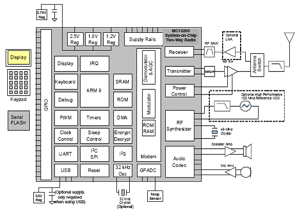
图.MC13260 SoC双向无线电参考设计
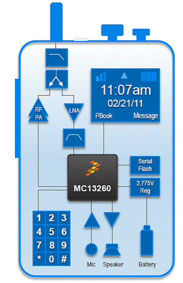
图3.MC13260 SoC双向无线电系统框图
责任编辑:HanFeng
【免责声明】
1、本文内容、数据、图表等来源于网络引用或其他公开资料,版权归属原作者、原发表出处。若版权所有方对本文的引用持有异议,请联系拍明芯城(marketing@iczoom.com),本方将及时处理。
2、本文的引用仅供读者交流学习使用,不涉及商业目的。
3、本文内容仅代表作者观点,拍明芯城不对内容的准确性、可靠性或完整性提供明示或暗示的保证。读者阅读本文后做出的决定或行为,是基于自主意愿和独立判断做出的,请读者明确相关结果。
4、如需转载本方拥有版权的文章,请联系拍明芯城(marketing@iczoom.com)注明“转载原因”。未经允许私自转载拍明芯城将保留追究其法律责任的权利。
拍明芯城拥有对此声明的最终解释权。
相关资讯
:
基于MC33771主控芯片的新能源锂电池管理系统解决方案

AMIC110 32位Sitara ARM MCU开发方案

基于AMIC110多协议可编程工业通信处理器的32位Sitara ARM MCU开发方案

基于展讯SC9820超低成本LTE芯片平台的儿童智能手表解决方案

基于TI公司的AM437x双照相机参考设计

基于MTK6580芯片的W2智能手表解决方案


 2012- 2022 拍明芯城ICZOOM.com 版权所有 客服热线:400-693-8369 (9:00-18:00)


