


 产品分类
产品分类
Microchip和Digilent dsPIC33F Cerebot MC7马达控制方案
 76
76
 拍明
拍明
原标题:Microchip和Digilent dsPIC33F Cerebot MC7马达控制方案
microchip公司的dsPIC33F系列是高性能16位数字信号控制器(DSC),采用改进的哈佛架构,高达40MIPS,16位数据通路,24位指令,工作电压 3.0-3.6V,主要用在各种马达控制如无刷DC马达,单相和三相马达与开关磁阻电动机。此外也可用在UPS,逆变器,开关电源,功率因素修正以及服务器,通信设备和其它工业设备的电源管理模块。本文介绍了dsPIC33F主要特性,方框图以及Cerebot MC7马达控制板主要特性,方框图和电路图。
The dsPIC33FJXXXMCX06A/X08A/X10A family of devices supports a variety of motor control applications, such as brushless DC motors, single and 3-phase induction motors and switched reluctance motors. The dsPIC33F Motor Control products are also well-suited for Uninterrupted Power Supply (UPS), inverters, Switched mode power supplies, power factor correction and also for controlling the power management module in servers, telecommunication equipment and other industrial equipment.
dsPIC33F主要特性:
Operating Range:
• Up to 40 MIPS operation (@ 3.0-3.6V):
- Industrial temperature range (-40 ℃ to +85℃)
- Extended temperature range (-40℃ to +125℃)
• Up to 20 MIPS operation (@ 3.0-3.6V):
- High temperature range (-40℃ to +150℃)
High-Performance DSC CPU:
• Modified Harvard architecture
• C compiler optimized instruction set
• 16-bit wide data path
• 24-bit wide instructions
• Linear program memory addressing up to 4M instruction words
• Linear data memory addressing up to 64 Kbytes
• 83 base instructions: mostly 1 word/1 cycle
• Two 40-bit accumulators:
- With rounding and saturation options
• Flexible and powerful addressing modes:
- Indirect, Modulo and Bit-Reversed
• Software stack
• 16 x 16 fractional/integer multiply operations
• 32/16 and 16/16 divide operations
• Single-cycle multiply and accumulate:
- Accumulator write back for DSP operations
- Dual data fetch
• Up to ±16-bit shifts for up to 40-bit data
Direct Memory Access (DMA):
• 8-channel hardware DMA
• 2 Kbytes dual ported DMA buffer area (DMA RAM) to store data transferred via DMA:
- Allows data transfer between RAM and a peripheral while CPU is executing code (no cycle stealing)
• Most peripherals support DMA
Interrupt Controller:
• 5-cycle latency
• Up to 67 available interrupt sources
• Up to five external interrupts
• Seven programmable priority levels
• Five processor exceptions
Digital I/O:
• Up to 85 programmable digital I/O pins
• Wake-up/Interrupt-on-Change on up to 24 pins
• Output pins can drive from 3.0V to 3.6V
• Up to 5.5V output with open drain configuration on 5V tolerant pins with an external pull-up
• 4 mA sink on all I/O pins
On-Chip Flash and SRAM:
• Flash program memory, up to 256 Kbytes
• Data SRAM, up to 30 Kbytes (includes 2 Kbytes of DMA RAM)
System Management:
• Flexible clock options:
- External, crystal, resonator, internal RC
- Fully integrated PLL
- Extremely low jitter PLL
• Power-up Timer
• Oscillator Start-up Timer/Stabilizer
• Watchdog Timer with its own RC oscillator
• Fail-Safe Clock Monitor (FSCM)
• Reset by multiple sources
Power Management:
• On-chip 2.5V voltage regulator
• Switch between clock sources in real time
• Idle, Sleep and Doze modes with fast wake-up
Timers/Capture/Compare/PWM:
• Timer/Counters, up to nine 16-bit timers:
- Can pair up to make four 32-bit timers
- 1 timer runs as Real-Time Clock (RTC) with external 32.768 kHz oscillator
- Programmable prescaler
• Input Capture (up to eight channels):
- Capture on up, down or both edges
- 16-bit capture input functions
- 4-deep FIFO on each capture
• Output Compare (up to eight channels):
- Single or Dual 16-bit Compare mode
- 16-bit Glitchless PWM mode
Communication Modules:
• 3-wire SPI (up to two modules):
- Framing supports I/O interface to simple codecs
- Supports 8-bit and 16-bit data
- Supports all serial clock formats and sampling modes
• I2C™ (up to 2 modules):
- Full Multi-Master Slave mode support
- 7-bit and 10-bit addressing
- Bus collision detection and arbitration
- Integrated signal conditioning
- Slave address masking
• UART (up to 2 modules):
- Interrupt on address bit detect
- Interrupt on UART error
- Wake-up on Start bit from Sleep mode
- 4-character TX and RX FIFO buffers
- LIN/J2602 support
- IrDA® encoding and decoding in hardware
- High-Speed Baud mode
- Hardware flow control with CTS and RTS
• Enhanced CAN (ECAN™ technology) 2.0B active (up to 2 modules):
- Up to 8 transmit and up to 32 receive buffers
- 16 receive filters and three masks
- Loopback, Listen Only and Listen All Messages modes for diagnostics and bus monitoring
- Wake-up on CAN message
- Automatic processing of Remote Transmission Requests
- FIFO mode using DMA
- DeviceNet™ addressing support
Motor Control Peripherals:
• Motor Control PWM (up to eight channels):
- Four duty cycle generators
- Independent or Complementary mode
- Programmable dead time and output polarity
- Edge or center-aligned
- Manual output override control
- Up to two Fault inputs
- Trigger for ADC conversions
- PWM frequency for 16-bit resolution (@ 40 MIPS) = 1220 Hz for Edge-Aligned mode, 610 Hz for Center-Aligned mode
- PWM frequency for 11-bit resolution (@ 40 MIPS) = 39.1 kHz for Edge-Aligned mode, 19.55 kHz for Center-Aligned mode
• Quadrature Encoder Interface (QEI) module:
- Phase A, Phase B and index pulse input
- 16-bit up/down position counter
- Count direction status
- Position Measurement (x2 and x4) mode
- Programmable digital noise filters on inputs
- Alternate 16-Bit Timer/Counter mode
- Interrupt on position counter rollover/underflow
Analog-to-Digital Converters (ADCs):
• Up to two ADC modules in a device
• 10-bit, 1.1 Msps or 12-bit, 500 Ksps conversion:
- Two, four or eight simultaneous samples
- Up to 32 input channels with auto-scanning
- Conversion start can be manual or synchronized with one of four trigger sources
- Conversion possible in Sleep mode
- ±1 LSb max integral nonlinearity
- ±1 LSb max differential nonlinearity
CMOS Flash Technology:
• Low-power, high-speed Flash technology
• Fully static design
• 3.3V (±10%) operating voltage
• Industrial and extended temperature
• Low-power consumption
Packaging:
• 100-pin TQFP (14x14x1 mm and 12x12x1 mm)
• 80-pin TQFP (12x12x1 mm)
• 64-pin TQFP (10x10x1 mm)
• 64-pin QFN (9x9x0.9 mm)
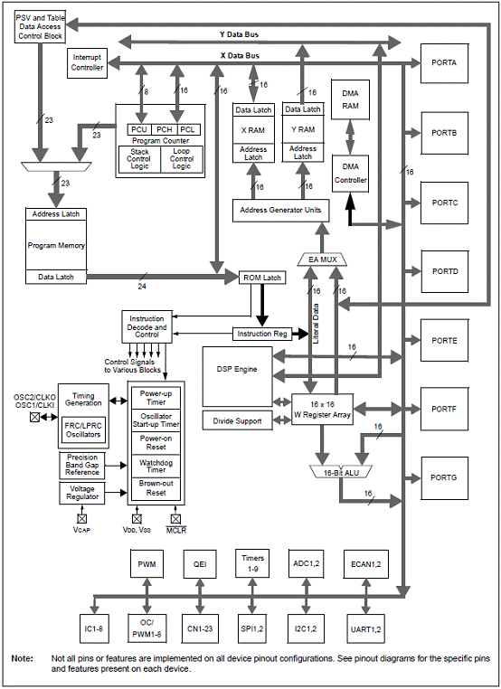
图1。dsPIC33F系列方框图
Cerebot MC7马达控制板
The Cerebot MC7 board is microcontroller development board based on a Microchip dsPIC 16-bit Digital Signal Controller.
The Cerebot MC7 is primarily intended to be used as a controller for electro-mechanical devices such as DC motors. The microcontroller used, a dsPIC33FJ128MC706A, is a member of a dsPIC family optimized for motor control applications.
The Cerebot MC7 provides four Half-Bridge circuits that are rated for 24V at up to 5A. Each of these Half Bridge circuits is connected to the dsPIC A/D converter to measure voltage and current for closed loop feedback control. These half bridges can be used to control two brushed DC motors, two bi-polar stepper motors, one brushless DC motor, one uni-polar stepper motor. In addition, the board can be used to implement controllers for switched DCDC converters.
The Cerebot MC7 works with the Microchip MPLAB® development environment and provides built in programming and debugging support within the MPLAB® IDE.
Cerebot MC7马达控制板主要特性:
a dsPIC33FJ128MC706A microcontroller
four 24V/5A Half Bridge circuits with current and voltage feedback and provision for over-current interrupt
power supply voltage up to 24V
5V/4A switching power supply
integrated programming/debugging circuit
one CAN network interface
three Pmod connectors for Digilent peripheral module boards
eight RC servo connectors
two I2C daisy chain connectors
256Kbit I2C EEPROM
two push buttons and four LEDs
ESD protection and short circuit protection for all I/O pins.
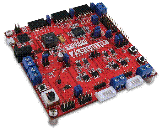
图2。Cerebot MC7马达控制板外形图
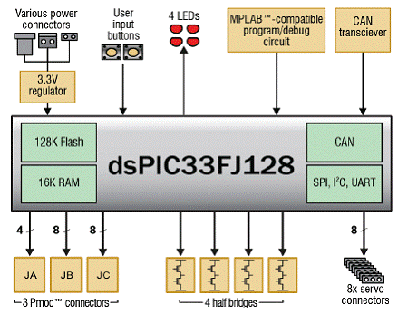
图3。Cerebot MC7马达控制板框图
责任编辑:HanFeng
【免责声明】
1、本文内容、数据、图表等来源于网络引用或其他公开资料,版权归属原作者、原发表出处。若版权所有方对本文的引用持有异议,请联系拍明芯城(marketing@iczoom.com),本方将及时处理。
2、本文的引用仅供读者交流学习使用,不涉及商业目的。
3、本文内容仅代表作者观点,拍明芯城不对内容的准确性、可靠性或完整性提供明示或暗示的保证。读者阅读本文后做出的决定或行为,是基于自主意愿和独立判断做出的,请读者明确相关结果。
4、如需转载本方拥有版权的文章,请联系拍明芯城(marketing@iczoom.com)注明“转载原因”。未经允许私自转载拍明芯城将保留追究其法律责任的权利。
拍明芯城拥有对此声明的最终解释权。
相关资讯
:
基于MC33771主控芯片的新能源锂电池管理系统解决方案

AMIC110 32位Sitara ARM MCU开发方案

基于AMIC110多协议可编程工业通信处理器的32位Sitara ARM MCU开发方案

基于展讯SC9820超低成本LTE芯片平台的儿童智能手表解决方案

基于TI公司的AM437x双照相机参考设计

基于MTK6580芯片的W2智能手表解决方案


 2012- 2022 拍明芯城ICZOOM.com 版权所有 客服热线:400-693-8369 (9:00-18:00)


