


 产品分类
产品分类
TI MSP430x461x1智能水表和煤气表解决方案
 114
114
 拍明
拍明
原标题:TI MSP430x461x1智能水表和煤气表解决方案
TI公司的智能水表和煤气表解决方案采用MSP430 16位超低功耗MCU MSP430x461x1, 2.4 GHz Zigbee 和802.15.4解决方案CC2510Fx/CC2511Fx,小于1GHz RF器件CC1110Fx/CC1111Fx, 850 – 950 MHz RF前端器件CC1190,以及RFID 预付费解决方案TRF7960/61和超低静态系统电源LM2840, LM2841或LM2842,马达驱动器与温度传感器TMP105等.本文介绍了智能水表和煤气表解决方案方框图和设计考虑以及主要器件的主要特性.
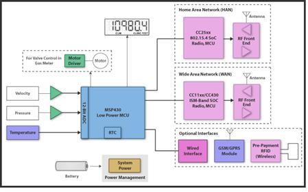
图1.智能水表和煤气表解决方案方框图
智能水表和煤气表设计考虑
Gas and Water AMR (Automated Meter Reading) is an electronic metering (e-meter) technology that includes both the metrology and a one-way communication medium that collects and presents time synchronized interval meter data to utilities and provides usage profiles of customers’ consumption over time. It combines high powered end points, network collectors, a data collection engine and fixed network technology to enable providers to know who is using how much gas and when.
Gas and Water AMI (Advanced Metering Infrastructure), sometimes referred to as smart metering, is a two way communications network that adds additional communication and control capability to AMR that can include valve control and customer access to consumption data.
TI provides a broad portfolio of high-performance products that support many key features necessary for today’s AMR and AMI Smart Gas and Water Meters (from ultrasonic to mechanical).
TI智能水表和煤气表解决方案主要特性:
1)Two-way Communication and Time Synchronized Measurement
TI provides the Low Power RF portfolio (both sub-1 GHz and 2.4 GHz solutions) that interface with a TI MCU. This type of communication enables early leak detection in these meters as well as monitoring and customer awareness
2)Logging and Billing
With the implementation of flexible tariff rates it is critical to have a system where consumption information is logged. TI MCU solutions provide embedded flash technology to make this type of system a reality. In addition, TI provides solutions for anti-tamper and pre-payment RFID options for the ultimate in flexibility in today’s smart gas meters.
3)Infrastructure life-time extension
In order to optimize service frequency, battery life times in this type of application need to last 10-15 years. TI’s MSP430 Ultra Low Power MCU’s fit seamlessly into this thought process by combining high-performance with low power.
4)Power
As part of maximizing battery life, the correct selection of an ultra-low quiescent current power management device is a key to optimizing the low power of the MSP430. While running the MCU directly from the battery may work (within the specified MCU operating range) and seem to save the cost of power management components, the lack of voltage regulation means much higher MCU stand-by power consumption and lower battery life. This can lead to higher maintenance costs that will far offset any cost savings observed by eliminating the regulator. Regulating the MCU and peripheral communication ICs at the lowest possible voltage will optimize power savings and lengthen battery life.
Depending on the type of battery used and the operating mode (full load) duty cycle of the meter, there are multiple choices in power management solutions. For simple, low duty cycle (long stand-by) applications, using batteries with a fairly flat discharge curve (such as primary cell Li-SOCl2) the use of ultra-low Iq LDOs can provide long battery life at very low cost. For higher operating duty cycle applications, the use of a low Iq DCDC regulator with power savings mode (for light loads) provides higher efficiency with a modest increase in cost.
For applications using batteries with a linear discharge curve, such as multi-cell alkaline or NiXX, the use of a low-Iq buck/boost converter will maximize battery life by providing regulation down to discharge voltages as low as 1.8-volts. For use of single-cell or small coin cell batteries, where the battery voltage can be less than the regulated voltage, the use of low-Iq boost converters can provide regulation with input voltages as low as 0.7-volts.
Although full operation of the MCU and peripheral communication ICs can be optimized at one voltage, in stand-by mode, these devices can operate at much lower voltages (simply maintaining RTC and memory). The use of DCDC converters and LDOs with dynamic voltage scaling (usually implemented with a V-Select logic pin) can further increase battery life.
5)Analog Sensing
The mechanical forces in gas meters are measured/detected by inductive sensors (flow), pressure sensors, and RTD or silicon temp sensors (temperature). Because voltages are very low, precise low-noise amplifiers (for flow and temperature), and instrumentation amps (for pressure) such as the OPA2209 and INA10x, respectively, are needed at the front end. Usually the voltage is digitized with precision ADCs which are integrated in the MSP430.
Ultrasonic meters have a much simpler mechanical structure than diaphragm meters; this leads to lighter and more compact design. They detect smaller leaks and quicker than diaphragm meters thanks to their specific measurement method which leads to a wider range measurement. Ultrasonic meters require specific analog front end for flow detection proportional to the time measurement and its accuracy between the two ultrasonic sensors. TI is currently developing devices which will enable measurement precision to go as low as several picoseconds and will seamlessly interface to the MSP430.
By supporting such features TI enables you to prepare accurate bills, perform regular gas system balances and reconciliation, enable early leak detection, and provide real-time usage information for optimal energy savings.
智能水表和煤气表所采用的主要元器件:
1) MSP430 16-bit Ultra-Low Power MCU’s
TI’s MSP430 has the performance to execute Smart Gas and Water Meter objectives. This includes: two-way communication for frequent remote reading, embedded flash technology for water consumption information logging, and multiple interfaces for pre-payment and anti-tampering options. All of these features are included in an ultra low-power MCU to extend water meter infrastructure lifetime.
MSP430F4619 :16-Bit Ultra-Low-Power MCU, 120KB Flash, 4KB RAM, 12-Bit ADC, DMA, 160 Seg LCD
The Texas Instruments MSP430 family of ultralow-power microcontrollers consists of several devices featuring different sets of peripherals targeted for various applications. The architecture, combined with five low-power modes, is optimized to achieve extended battery life in portable measurement applications. The devices feature a powerful 16-bit RISC CPU, 16-bit registers, and constant generators that contribute to maximum code
efficiency. The digitally controlled oscillator (DCO) allows wake-up from low-power modes to active mode in less than 6 s.
The MSP430x461x(1) series are microcontroller configurations with two 16-bit timers, a high-performance 12-bit A/D converter (MSP430x461x only), one universal serial communication interface (USCI), one universal synchronous/asynchronous communication interface (USART), DMA, 80 I/O pins, and a liquid crystal display (LCD) driver with regulated charge pump. Typical applications for this device include portable medical applications and e-meter applications.
MSP430F4619主要特性:
_ Low Supply Voltage Range: 1.8 V to 3.6 V
_ Ultralow-Power Consumption:
− Active Mode: 400 uA at 1 MHz, 2.2 V
− Standby Mode: 1.3uA
− Off Mode (RAM Retention): 0.22uA
_ Five Power-Saving Modes
_ Wake-Up From Standby Mode in Less Than 6 us
_ 16-Bit RISC Architecture, Extended
Memory, 125-ns Instruction Cycle Time
_ Three Channel Internal DMA
_ 12-Bit A/D Converter With Internal
Reference, Sample-and-Hold and Autoscan
Feature (MSP430x461x only)
_ 16-Bit Timer_A With Three
Capture/Compare Registers
_ 16-Bit Timer_B With Seven
Capture/Compare-With-Shadow Registers
_ On-Chip Comparator
_ Supply Voltage Supervisor/Monitor With
Programmable Level Detection
_ Basic Timer With Real Time Clock Feature
_ Integrated LCD Driver up to 160 Segments With Regulated Charge Pump
_ Serial Communication Interface (USART1),
Select Asynchronous UART or
Synchronous SPI by Software
_ Universal Serial Communication Interface
− Enhanced UART Supporting
Auto-Baudrate Detection
− IrDA Encoder and Decoder
− Synchronous SPI
− I2CTM
_ Serial Onboard Programming,
Programmable Code Protection by Security Fuse
_ Brownout Detector
_ Family Members Include:
− MSP430x4616, MSP430x46161†:
92KB+256B Flash or ROM Memory
4KB RAM
− MSP430x4617, MSP430x46171†:
92KB+256B Flash or ROM Memory,
8KB RAM
− MSP430x4618, MSP430x46181†:
116KB+256B Flash or ROM Memory,
8KB RAM
− MSP430x4619, MSP430x46191†:
120KB+256B Flash or ROM Memory,
4KB RAM
_ For Complete Module Descriptions
All MSP430 microcontrollers include an Embedded Emulation Module (EEM) allowing advanced debugging and programming through easy to use development tools. Recommended hardware options include the following:
_ Debugging and Programming Interface
− MSP-FET430UIF (USB)
− MSP-FET430PIF (Parallel Port)
_ Debugging and Programming Interface with Target Board
− MSP-FET430U100
_ Stand-Alone Target Board
− MSP-TS430PZ100
_ Production Programmer
− MSP-GANG430
详见:
http://www.ti.com/lit/ds/symlink/msp430f4619.pdf
2) 2.4 GHz Solutions (Zigbee and 802.15.4)
The CC2510Fx/CC2511Fx is a true low-cost 2.4 GHz system-on-chip (SoC) designed for lowpower wireless applications. The CC2510Fx/CC2511Fx combines the excellent performance of the state-of-the-art RF transceiver CC2500 with an industry-standard enhanced 8051 MCU, up to 32 kB of in-system programmable flash memory and 4 kB of RAM, and many other powerful features. The small 6x6 mm package makes it very suited for applications with size limitations.
The CC2510Fx/CC2511Fx is highly suited for systems where very low power consumption is required. This is ensured by several advanced low-power operating modes. The CC2511Fx adds a full-speed USB controller to the feature set of the CC2510Fx. Interfacing to a PC using the USB interface is quick and easy, and the high data rate (12 Mbps) of the USB interface avoids the bottlenecks of RS-232 or low-speed
USB interfaces.
CC2510Fx/CC2511Fx 主要特性:
• Radio
o High-performance RF transceiver based on the market-leading CC2500
o Excellent receiver selectivity and blocking performance
o High sensitivity (−103 dBm at 2.4 kBaud)
o Programmable data rate up to 500 kBaud
o Programmable output power up to 1 dBm for all supported frequencies
o Frequency range: 2400 - 2483.5 MHz
o Digital RSSI / LQI support
• Current Consumption
o Low current consumption (RX: 17.1 mA @2.4 kBaud, TX: 16 mA @ −6 dBm output power)
o 0.3 μA in PM3 (the operating mode with the lowest power consumption)
• MCU, Memory, and Peripherals
o High performance and low power 8051 microcontroller core.
o 8/16/32 kB in-system programmable flash, and 1/2/4 kB RAM
o Full-Speed USB Controller with 1 kB USB FIFO (CC2511Fx )
o I2S interface
o 7 - 12 bit ADC with up to eight inputs
o 128-bit AES security coprocessor
o Powerful DMA functionality
o Two USARTs
o 16-bit timer with DSM mode
o Three 8-bit timers
o Hardware debug support
o 21 (CC2510Fx ) or 19 (CC2511Fx ) GPIO pins
• General
o Wide supply voltage range (2.0V - 3.6V)
o Green package: RoHS compliant and no antimony or bromine, 6x6mm QFN 36
详见:
http://www.ti.com/lit/ds/symlink/cc2510f32.pdf
3) Sub 1-Ghz Solutions
The CC1110Fx/CC1111Fx is a true low-power sub-1 GHz system-on-chip (SoC) designed for lowpowerwireless applications. TheCC1110Fx/CC1111Fx combines the excellent performance of the state-of-the-art RF transceiver CC1101 with an industry-standard enhanced 8051 MCU, up to 32 kB of in-system programmable flash memory and up to 4 kB of RAM, and many other powerful features. The small 6x6 mm package makes it very suited for applications with size limitations.
The CC1110Fx/CC1111Fx is highly suited for systems where very low power consumption is required. This is ensured by several advanced low-power operating modes. The CC1111Fx adds a full-speed USB 2.0 interface to the feature set of the CC1110Fx. Interfacing to a PC using the USB interface is quick and easy, and the high data rate (12 Mbps) of the USB interface avoids the bottlenecks of RS-232 or low-speed USB interfaces.
CC1110Fx/CC1111Fx 主要特性:
Radio
o High-performance RF transceiver based on the market-leading CC1101
o Excellent receiver selectivity and blocking performance
o High sensitivity (−110
o dBm at 1.2 kBaud)
o Programmable data rate up to 500 kBaud
o Programmable output power up to 10 dBm for all supported frequencies
o Frequency range: 300 - 348 MHz, 391 – 464 MHz and 782 - 928 MHz
o Digital RSSI / LQI support Low Power
o Low current consumption (RX: 16.2 mA @ 1.2 kBaud, TX: 15.2 mA @ −6 dBm output power)
o 0.3 μA in PM3 (the operating mode with the lowest power consumption)
o 0.5 μA in PM2 (operating mode with the second lowest power consumption, timer or external interrupt wakeup)MCU, Memory, and Peripherals
o High performance and low power 8051 microcontroller core.
o Powerful DMA functionality
o 8/16/32 KB in-system programmable flash, and 1/2/4 KB RAM
o Full-Speed USB Controller with 1 KB FIFO (CC1111Fx )
o 128-bit AES security coprocessor
o 7 - 12 bit ADC with up to eight inputs
o I2S interface
o Two USARTs
o 16-bit timer with DSM mode
o Three 8-bit timers
o Hardware debug support
o 21 (CC1110Fx ) or 19 (CC1111Fx ) GPIO pins
o SW compatible with CC2510Fx/CC2511Fx General
o Wide supply voltage range (2.0V - 3.6V)
o RoHS compliant 6x6 mm QFN 36 package
详见:
http://www.ti.com/lit/ds/symlink/cc1110f32.pdf
4) 850 – 950 MHz RF Front End
CC1190 is a cost-effective and high-performance RF Front End for low-power and low-voltage wireless applications at 850 - 950 MHz.
CC1190 is a range extender for the sub-1 GHz low-power RF transceivers, transmitters, and System-on-Chip devices from Texas Instruments.
CC1190 integrates a power amplifier (PA), a low-noise amplifier (LNA), switches, and RF matching for the design of a high-performance wireless systems.
CC1190 increases the link budget by providing a power amplifier for increased output power, and an LNA with low noise figure for improved receiver sensitivity.
CC1190 provides an efficient and easy-to-use range extender in a compact 4-mm × 4-mm QFN-16 package.
CC1190主要特性:
Seamless Interface to Sub-1 GHz Low Power RF Devices from Texas Instruments Up to 27 dBm (0.5 W) Output Power
6 dB Typical Sensitivity Improvement with CC11xx and CC430
Few External Components
Integrated PA
Integrated LNA
Integrated Switches
Integrated Matching Network
Integrated Inductors
Digital Control of LNA and PA Gain by HGM Pin
50-nA in Power Down (LNA_EN = PA_EN = 0)
High Transmit Power Efficiency
PAE = 50% at 26 dBm Output Power
Low Receive Current Consumption
3 mA for High Gain Mode
26 µA for Low Gain Mode
2.9 dB LNA Noise Figure, Including Switch and External Antenna Match
RoHS Compliant 4-mm × 4-mm QFN-16 Package
2 V to 3.7 V Operation
详见:
http://www.ti.com/lit/ds/symlink/cc1190.pdf
5) RFID 预付费解决方案
TRF7960/61:Multi-Standard Fully Integrated 13.56-MHz RFID AFE and Data Framing Reader System
The TRF7960/61 is an integrated analog front end and data-framing system for a 13.56-MHz RFID reader system. Built-in programming options make it suitable for a wide range of applications for proximity and vicinity RFID systems.
The reader is configured by selecting the desired protocol in the control registers. Direct access to all control registers allows fine tuning of various reader parameters as needed.
TRF7960/61主要特性:
Completely Integrated Protocol Handling
Separate Internal High-PSRR Power Supplies for Analog, Digital, and PA Sections
Provide Noise Isolation for Superior Read Range and Reliability
Dual Receiver Inputs With AM and PM Demodulation to Minimize Communication Holes
Receiver AM and PM RSSI
Reader-to-Reader Anti-Collision
High Integration Reduces Total BOM and Board Area
Single External 13.56-MHz Crystal Oscillator
MCU-Selectable Clock-Frequency Output of RF, RF/2, or RF/4
Adjustable 20-mA, High-PSRR LDO for Powering External MCU
Easy to Use With High Flexibility
Auto-Configured Default Modes for Each Supported ISO Protocol
12 User-Programmable Registers
Selectable Receiver Gain and AGC
Programmable Output Power (100 mW or 200 mW)
Adjustable ASK Modulation Range (8% to 30%)
Built-In Receiver Band-Pass Filter With User-Selectable Corner Frequencies
Wide Operating Voltage Range of 2.7 V to 5.5 V
Ultra-Low-Power Modes
Power Down < 1 µA
Standby 120 µA
详见:
http://www.ti.com/lit/ds/symlink/trf7960.pdf
6) Ultra-Low Quiescent System Power
The LM2840, LM2841 and LM2842 are PWM DC/DC buck (step-down) regulators. With a wide input range from 4.5V-42V, they are suitable for a wide range of applications such as power conditioning from unregulated sources. They feature a low RDSON (0.9Ω typical) internal switch for maximum efficiency (85% typical). Operating frequency is fixed at 550 kHz (X version) and 1.25 MHz (Y version) allowing the use of small external components while still being able to have low output voltage ripple. Soft-start can be implemented using the shutdown pin with an external RC circuit allowing the user to tailor the soft-start time to a specific application.
The LM2840 is optimized for up to 100 mA, the LM2841 for 300 mA and the LM2842 is optimized for up to 600 mA load currents. They all have a 0.765V nominal feedback voltage.
Additional features include: thermal shutdown, VIN under-voltage lockout, and gate drive under-voltage lockout. The LM2840, LM2841 and LM2842 are available in a low profile TSOT-6L package.
LM284x主要特性:
LM2840Q, LM2841Q and LM2842Q are Automotive Grade products that are AEC-Q100 grade 1 qualified (-40℃ to +125℃ operating junction temperature)
Input voltage range of 4.5V to 42V
Output current options of 100 mA, 300 mA and 600 mA
Feedback pin voltage of 0.765V
550 kHz (X) or 1.25 MHz (Y) switching frequency
Low shutdown IQ, 16 µA typical
Short circuit protected
Internally compensated
Soft-start circuitry
Small overall solution size (TSOT-6L package)
详见:
http://www.national.com/ds/LM/LM2841.pdf
7) Motor Driver DRV8x
2A Low Voltage Dual Brushed DC or Single Bipolar Stepper Motor Driver (PWM Ctrl)
The DRV8833 provides a dual bridge motor driver solution for toys, printers, and other mechatronic applications.
The device has two H-bridge drivers, and can drive two DC brush motors, a bipolar stepper motor, solenoids, or other inductive loads.
The output driver block of each H-bridge consists of N-channel power MOSFET’s configured as an H-bridge to drive the motor windings. Each H-bridge includes circuitry to regulate or limit the winding current.
With proper PCB design, each H-bridge of the DRV8833 is capable of driving up to 1.5-A RMS (or DC) continuously, at 25℃ with a VM supply of 5 V. It can support peak currents of up to 2 A per bridge. Current capability is reduced slightly at lower VM voltages.
DRV8833主要特性:
Dual-H-Bridge Current-Control Motor Driver
Capable of Driving Two DC Motors or One Stepper Motor
Low MOSFET On-Resistance:
HS + LS 360 mΩ
Output Current 1.5-A RMS, 2-A Peak per H-Bridge
(at VM = 5 V, 25℃)
Outputs Can Be Paralleled for 3-A RMS,
4-A Peak
Wide Power Supply Voltage Range:
2.7 V – 10.8 V
PWM Winding Current Regulation/Limiting
Thermally Enhanced Surface Mount Package
详见:
http://www.ti.com/lit/ds/symlink/drv8833.pdf
8) Temperature Sensor
The TMP105 is a two-wire, serial output temperature sensor available in a WCSP package. Requiring no external components, the TMP105 is capable of reading temperatures with a resolution of 0.0625°C.
The TMP105 features a Two-Wire interface that is SMBus-compatible, with the TMP105 allowing up to two devices on one bus. The TMP105 features an SMBus Alert function.
The TMP105 is ideal for extended temperature measurement in a variety of communication, computer, consumer, environmental, industrial, and instrumentation applications.
The TMP105 is specified for operation over a temperature range of –40℃ to +125℃.
TMP105主要特性:
• SUPPORTS 1.8V I2C™ BUS
• TWO ADDRESSES
• DIGITAL OUTPUT: Two-Wire Serial Interface
• RESOLUTION: 9- to 12-Bits, User-Selectable
• ACCURACY:
– ±2.0℃ (max) from –25℃ to +85℃
– ±3.0℃ (max) from –40℃ to +125℃
• LOW QUIESCENT CURRENT:
50μA, 1.5μA Standby
• NO POWER-UP SEQUENCE REQUIRED, I2C PULLUPS CAN BE ENABLED PRIOR TO V+
责任编辑:HanFeng
【免责声明】
1、本文内容、数据、图表等来源于网络引用或其他公开资料,版权归属原作者、原发表出处。若版权所有方对本文的引用持有异议,请联系拍明芯城(marketing@iczoom.com),本方将及时处理。
2、本文的引用仅供读者交流学习使用,不涉及商业目的。
3、本文内容仅代表作者观点,拍明芯城不对内容的准确性、可靠性或完整性提供明示或暗示的保证。读者阅读本文后做出的决定或行为,是基于自主意愿和独立判断做出的,请读者明确相关结果。
4、如需转载本方拥有版权的文章,请联系拍明芯城(marketing@iczoom.com)注明“转载原因”。未经允许私自转载拍明芯城将保留追究其法律责任的权利。
拍明芯城拥有对此声明的最终解释权。
相关资讯
:
基于MC33771主控芯片的新能源锂电池管理系统解决方案

AMIC110 32位Sitara ARM MCU开发方案

基于AMIC110多协议可编程工业通信处理器的32位Sitara ARM MCU开发方案

基于展讯SC9820超低成本LTE芯片平台的儿童智能手表解决方案

基于TI公司的AM437x双照相机参考设计

基于MTK6580芯片的W2智能手表解决方案


 2012- 2022 拍明芯城ICZOOM.com 版权所有 客服热线:400-693-8369 (9:00-18:00)


