


 产品分类
产品分类
Microchip连接电网的太阳能微逆变器220V参考设计
 116
116
 拍明
拍明
原标题:Microchip连接电网的太阳能微逆变器220V参考设计
microchip公司的连接电网的太阳能微逆变器参考设计(220V)采用dsPIC33FJx6GS系列产品.该16位数字信号控制器包括DSP功能和高性能16位微控制器(MCU)架构,3.0V-3.6V时的性能高达40MIPS.太阳能微逆变器系数的峰值效率高达94%,输出电流的THD小于5%,功率因素大于0.95,具有最大功率点跟踪(MPPT),全数字控制,太阳能电池板的电压从25V到55VDC,MPPT电压25V-45V,最大DC短路电流10A,广泛用于连接电网农村家庭太阳能系统.本文介绍了dsPIC33FJx6GS系列主要特性,方框图,CPU核方框图,太阳能微逆变器参考设计框图,电路图和材料清单与 PCB布局图.
dsPIC33FJ06GS101/X02 and dsPIC33FJ16GSX02/X04 devices contain extensive Digital Signal Processor (DSP) functionality with a high-performance, 16-bit microcontroller (MCU) architecture.
dsPIC33FJx6GS系列主要特性:
Operating Range:
• Up to 40 MIPS Operation (at 3.0-3.6V):
- Industrial temperature range (-40℃ to +85℃)
- Extended temperature range (-40℃ to +125℃)
High-Performance DSC CPU:
• Modified Harvard Architecture
• C Compiler Optimized Instruction Set
• 16-Bit Wide Data Path
• 24-Bit Wide Instructions
• Linear Program Memory Addressing up to 4M Instruction Words
• Linear Data Memory Addressing up to 64 Kbytes
• 83 Base Instructions: Mostly 1 Word/1 Cycle
• Two 40-Bit Accumulators with Rounding and Saturation Options
• Flexible and Powerful Addressing modes:
- Indirect
- Modulo
- Bit-Reversed
• Software Stack
• 16 x 16 Fractional/Integer Multiply Operations
• 32/16 and 16/16 Divide Operations
• Single-Cycle Multiply and Accumulate:
- Accumulator write back for DSP operations
- Dual data fetch
• Up to ±16-Bit Shifts for up to 40-Bit Data
Digital I/O:
• Peripheral Pin Select Functionality
• Up to 35 Programmable Digital I/O Pins
• Wake-up/Interrupt-on-Change for up to 30 Pins
• Output Pins can Drive Voltage from 3.0V to 3.6V
• Up to 5V Output with Open-Drain Configuration
• 5V Tolerant Digital Input Pins (except RB5)
• 16 mA Source/Sink on All PWM pins
On-Chip Flash and SRAM:
• Flash Program Memory (up to 16 Kbytes)
• Data SRAM (up to 2 Kbytes)
• Boot and General Security for Program Flash
Peripheral Features:
• Timer/Counters, up to Three 16-Bit Timers:
- Can pair up to make one 32-bit timer
• Input Capture (up to two channels):
- Capture on up, down or both edges
- 16-bit capture input functions
- 4-deep FIFO on each capture
• Output Compare (up to two channels):
- Single or Dual 16-Bit Compare mode
- 16-Bit Glitchless PWM mode
• 4-Wire SPI:
- Framing supports I/O interface to simple codecs
- 1-deep FIFO Buffer.
- Supports 8-bit and 16-bit data
- Supports all serial clock formats and sampling modes
• I2C™:
- Supports Full Multi-Master Slave mode
- 7-bit and 10-bit addressing
- Bus collision detection and arbitration
- Integrated signal conditioning
- Slave address masking
• UART:
- Interrupt on address bit detect
- Interrupt on UART error
- Wake-up on Start bit from Sleep mode
- 4-character TX and RX FIFO buffers
- LIN bus support
- IrDA® encoding and decoding in hardware
- High-Speed Baud mode
- Hardware Flow Control with CTS and RTS
Interrupt Controller:
• 5-Cycle Latency
• Up to 35 Available Interrupt Sources
• Up to Three External Interrupts
• Seven Programmable Priority Levels
• Four Processor Exceptions
High-Speed PWM Module Features:
• Up to Four PWM Generators with Four to Eight Outputs
• Individual Time Base and Duty Cycle for each of the Eight PWM Outputs
• Dead Time for Rising and Falling Edges
• Duty Cycle Resolution of 1.04 ns
• Dead-Time Resolution of 1.04 ns
• Phase Shift Resolution of 1.04 ns
• frequency Resolution of 1.04 ns
• PWM modes Supported:
- Standard Edge-Aligned
- True Independent Output
- Complementary
- Center-Aligned
- Push-Pull
- Multi-Phase
- Variable Phase
- Fixed Off-Time
- Current Reset
- Current-Limit
• Independent Fault/Current-Limit Inputs for 8 PWM Outputs
• Output Override Control
• Special Event Trigger
• PWM Capture Feature
• Prescaler for Input Clock
• Dual Trigger from PWM to ADC
• PWMxL, PWMxH Output Pin Swapping
• PWM4H, PWM4L Pins Remappable
• On-the-Fly PWM Frequency, Duty Cycle and Phase Shift Changes
• Disabling of Individual PWM Generators
• Leading-Edge Blanking (LEB) Functionality High-Speed Analog Comparator
• Up to Four Analog Comparators:
- 20 ns response time
- 10-bit DAC for each analog comparator
- DACOUT pin to provide DAC output
- Programmable output polarity
- Selectable input source
- ADC sample and convert capability
• PWM Module Interface:
- PWM duty cycle control
- PWM period control
- PWM Fault detect High-Speed 10-Bit ADC
• 10-Bit Resolution
• Up to 12 Input Channels Grouped into Six Conversion Pairs
• Two Internal Reference Monitoring Inputs Grouped into a Pair
• Successive Approximation Register (SAR) Converters for Parallel Conversions of Analog Pairs:
- 4 Msps for devices with two SARs
- 2 Msps for devices with one SAR
• Dedicated Result Buffer for each Analog Channel
• Independent Trigger Source Section for each Analog Input Conversion Pair
Power Management:
• On-Chip 2.5V Voltage Regulator
• Switch between Clock Sources in Real Time
• Idle, Sleep, and Doze modes with Fast Wake-up
CMOS Flash Technology:
• Low-Power, High-Speed Flash Technology
• Fully Static Design
• 3.3V (±10%) Operating Voltage
• Industrial and Extended Temperature
• Low-Power Consumption
System Management:
• Flexible Clock Options:
- External, crystal, resonator, internal RC
- Phase-Locked Loop (PLL) with 120 MHz VCO
- Primary Crystal Oscillator (OSC) in the range of 3 MHz to 40 MHz
- Internal Low-Power RC (LPRC) oscillator at a frequency of 32 kHz
- Internal Fast RC (FRC) oscillator at a frequency of 7.37 MHz
• Power-on Reset (POR)
• Brown-out Reset (BOR)
• Power-up Timer (PWRT)
• Oscillator Start-up Timer (OST)
• Watchdog Timer with its RC Oscillator
• Fail-Safe Clock Monitor (FSCM)
• Reset by Multiple Sources
• In-Circuit Serial Programming™ (ICSP™)
• Reference Oscillator Output
Application Examples
• AC-to-DC Converters
• Automotive HID
• Battery Chargers
• DC-to-DC Converters
• Digital Lighting
• Induction Cooking
• LED Ballast
• Renewable Power/Pure Sine Wave Inverters
• Uninterruptible Power Supply (UPS) Packaging:
• 18-Pin SOIC
• 28-Pin SPDIP/SOIC/QFN-S
• 44-Pin TQFP/QFN
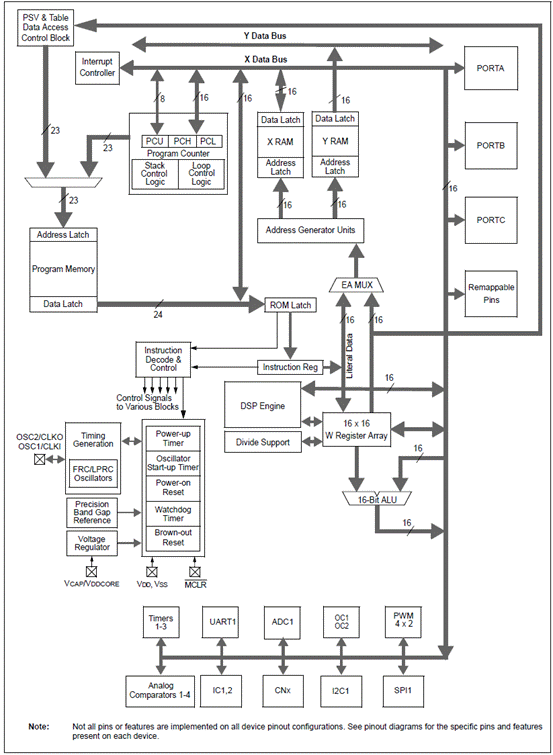
图1.dsPIC33FJx6GS系列方框图
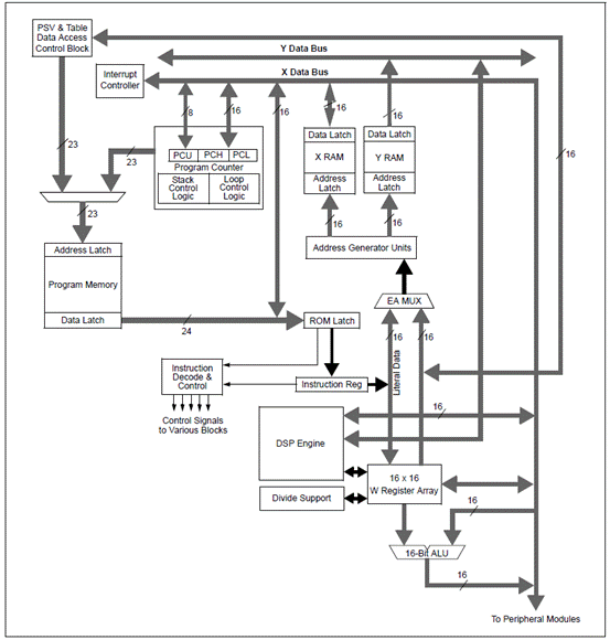
图2.dsPIC33FJx6GS系列CPU核方框图

图3.采用dsPIC33FJ16GS504的PFC 和三输出(12V,5V和3.3V)AC/DC电源框图
太阳能(光伏(PV))微逆变器参考设计
Due to global environmental concerns, photovoltaic (PV) systems (i.e., solar panels) are becoming more common as a renewable energy source.
The main drawbacks of PV energy are the high cost of manufacturing silicon solar panels and the low conversion efficiency. However, with the latest techniques in manufacturing, PV systems are becoming more efficient, as well as cost effective.
The conversion of the output voltage from a solar panel into usable DC or AC voltage must be done at its Maximum Power Point, or MPP. MPP is the PV output voltage at which the PV module delivers maximum energy to load.
Interfacing a solar inverter module with the power grid involves two major tasks. One is to ensure that the solar inverter module is operated at the Maximum Power Point (MPP). The second is to inject a sinusoidal current into the grid. Since the inverter is connected to the grid, the standards given by the utility companies must be obeyed. The EN61000-3-2, IEEE1547 standards, and the U.S. National Electrical Code (NEC) 690, are worth considering. These standards deal with issues like power quality, detection of islanding operation, grounding, and so on.
These inverters must be able to detect an islanding situation, and take appropriate action in order to prevent bodily harm and damage to equipment connected to the grid. Islanding is the continued operation of the inverter when the grid has been removed intentionally, by accident, or by damage. In other words, if the grid has been removed from the inverter; the inverter should then stop supplying power to the grid or energizing the grid.
The most common solar technologies today are the monocrystalline and multi-crystalline silicon modules.The MPP voltage range for these PV modules is normally defined in the range from 27V to 45V, at a power generation of approximate 200W, and their open-circuit voltage is below 45V.
In order to capture the maximum energy from the PV module, solar inverters must guarantee that the PV module is operated at the MPP. This is accomplished by the maximum power point control loop known as the Maximum Power Point Tracker (MPPT). It also involves PV output voltage ripple at the terminals of the PV module being sufficiently small, in order to operate around the MPP without too much variation in PV Current.

图3.农村家庭太阳能系统框图

图4.模块化逆变器(微逆变器)系统框图
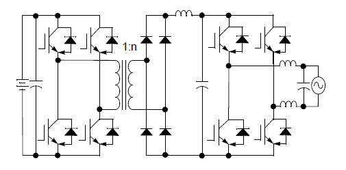
图5.太阳能微逆变器系统两级拓扑图
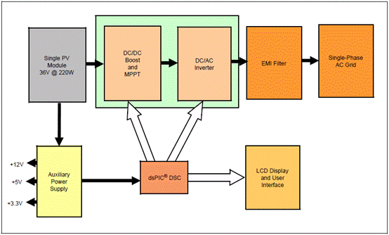
图6.太阳能微逆变器参考设计框图

图7.交错式反激转换器电路
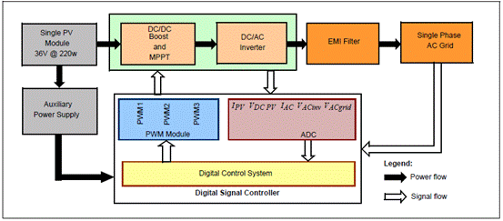
图8.连接电网的太阳能微逆变器框图
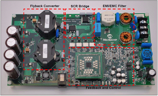
图9.连接电网的太阳能微逆变器参考设计板外形图
This reference design demonstrates the flexibility and power of SMPS dsPIC® Digital Signal Controllers in Grid connected power conversion systems. This reference design works with any photovoltaic (PV) panel of maximum 220 Watts having open circuit voltage between 25V to 55V DC. This reference design ensures maximum power tracking for PV panel voltage between 25V to 45V DC. Two versions of this reference design is available to support 110V and 220V Grid.
This reference design is implemented using a single dsPIC33F “GS” digital-power DSCs from Microchip that provides the full digital control of the power conversion and system management functions. As shown in this reference design the dsPIC33F ‘GS’ devices enable designers to easily and cost effectively create products using advanced switching techniques that lower switching losses and enable efficiencies as high as 94%. Grid-Connected Solar Micro Inverter Reference Design is royalty free when used in accordance with the licensing agreement.
太阳能微逆变器参考设计主要特性:
Peak efficiency of up to 94%
Beta build peak efficiency of up to 92%
Output current THD < 5%
Power factor >0.95
Maximum power point tracking
Grid voltage and frequency tracking
Protection against various current and voltage faults
System Islanding to detect grid failure
Full Digital Control
Specifications:
Micro Inverter for individual PV Module up to 220W
Wide PV Panel voltage : 25V to 55V DC
Maximum Power Point Tracking voltage: 25V to 45V
Maximum DC short circuit current : 10A
Grid Frequency range :
47 – 53 Hz for 220V systems
57 – 63 Hz for 110V systems
Grid voltage range :
90V – 140V for 110V systems
180V – 264V for 220V systems
责任编辑:HanFeng
【免责声明】
1、本文内容、数据、图表等来源于网络引用或其他公开资料,版权归属原作者、原发表出处。若版权所有方对本文的引用持有异议,请联系拍明芯城(marketing@iczoom.com),本方将及时处理。
2、本文的引用仅供读者交流学习使用,不涉及商业目的。
3、本文内容仅代表作者观点,拍明芯城不对内容的准确性、可靠性或完整性提供明示或暗示的保证。读者阅读本文后做出的决定或行为,是基于自主意愿和独立判断做出的,请读者明确相关结果。
4、如需转载本方拥有版权的文章,请联系拍明芯城(marketing@iczoom.com)注明“转载原因”。未经允许私自转载拍明芯城将保留追究其法律责任的权利。
拍明芯城拥有对此声明的最终解释权。
相关资讯
:
基于MC33771主控芯片的新能源锂电池管理系统解决方案

AMIC110 32位Sitara ARM MCU开发方案

基于AMIC110多协议可编程工业通信处理器的32位Sitara ARM MCU开发方案

基于展讯SC9820超低成本LTE芯片平台的儿童智能手表解决方案

基于TI公司的AM437x双照相机参考设计

基于MTK6580芯片的W2智能手表解决方案


 2012- 2022 拍明芯城ICZOOM.com 版权所有 客服热线:400-693-8369 (9:00-18:00)


