基于stm32f103rct6/stm32f103c6t6a/lsm6ds33/stp100n8f6的智能平衡车控制器方案
 138
138
 拍明
拍明
原标题:智能平衡车控制器方案
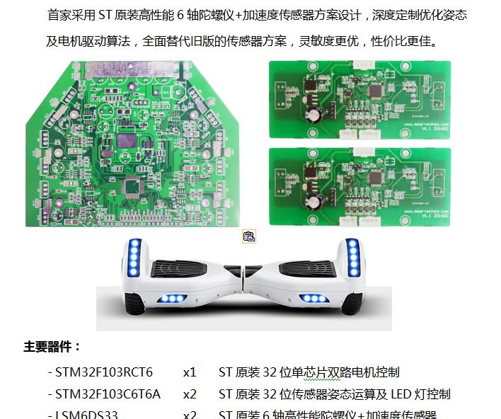
【stm32f103rct6】
Mainstream Performance line, ARM Cortex-M3 MCU with 256 Kbytes Flash, 72 MHz CPU, motor control, USB and CAN
The STM32F103xC, STM32F103xD and STM32F103xE performance line family incorporates the high-performance ARM® Cortex®-M3 32-bit RISC core operating at a 72 MHz frequency, high-speed embedded memories (Flash memory up to 512 Kbytes and SRAM up to 64 Kbytes), and an extensive range of enhanced I/Os and peripherals connected to two APB buses. All devices offer three 12-bit ADCs, four general-purpose 16-bit timers plus two PWM timers, as well as standard and advanced communication interfaces: up to two I2Cs, three SPIs, two I2Ss, one SDIO, five USARTs, an USB and a CAN.
The STM32F103xC/D/E high-density performance line family operates in the –40 to +105 °C temperature range, from a 2.0 to 3.6 V power supply. A comprehensive set of power-saving mode allows the design of low-power applications.
These features make the STM32F103xC/D/E high-density performance line microcontroller family suitable for a wide range of applications such as motor drives, application control, medical and handheld equipment, PC and gaming peripherals, GPS platforms, industrial applications, PLCs, inverters, printers, scanners, alarm systems video intercom, and HVAC.
主要特性
Core: ARM® 32-bit Cortex®-M3 CPU
72 MHz maximum frequency, 1.25 DMIPS/MHz (Dhrystone 2.1) performance at 0 wait state memory access
Single-cycle multiplication and hardware division
Memories
256 to 512 Kbytes of Flash memory
up to 64 Kbytes of SRAM
Flexible static memory controller with 4 Chip Select. Supports Compact Flash, SRAM, PSRAM, NOR and NAND memories
LCD parallel interface, 8080/6800 modes
Clock, reset and supply management
2.0 to 3.6 V application supply and I/Os
POR, PDR, and programmable voltage detector (PVD)
4-to-16 MHz crystal oscillator
Internal 8 MHz factory-trimmed RC
Internal 40 kHz RC with calibration
32 kHz oscillator for RTC with calibration
Low power
Sleep, Stop and Standby modes
VBAT supply for RTC and backup registers
3 × 12-bit, 1 μs A/D converters (up to 21 channels)
Conversion range: 0 to 3.6 V
Triple-sample and hold capability
Temperature sensor
2 × 12-bit D/A converters
DMA: 12-channel DMA controller
Supported peripherals: timers, ADCs, DAC, SDIO, I2Ss, SPIs, I2Cs and USARTs
Debug mode
Serial wire debug (SWD) & JTAG interfaces
Cortex®-M3 Embedded Trace Macrocell™
Up to 112 fast I/O ports
51/80/112 I/Os, all mappable on 16 external interrupt vectors and almost all 5 V-tolerant
Up to 11 timers
Up to four 16-bit timers, each with up to 4 IC/OC/PWM or pulse counter and quadrature (incremental) encoder input
2 × 16-bit motor control PWM timers with dead-time generation and emergency stop
2 × watchdog timers (Independent and Window)
SysTick timer: a 24-bit downcounter
2 × 16-bit basic timers to drive the DAC
Up to 13 communication interfaces
Up to 2 × I2C interfaces (SMBus/PMBus)
Up to 5 USARTs (ISO 7816 interface, LIN, IrDA capability, modem control)
Up to 3 SPIs (18 Mbit/s), 2 with I2S interface multiplexed
CAN interface (2.0B Active)
USB 2.0 full speed interface
SDIO interface
CRC calculation unit, 96-bit unique ID
ECOPACK® packages
电路原理图

【stm32f103c6t6a】
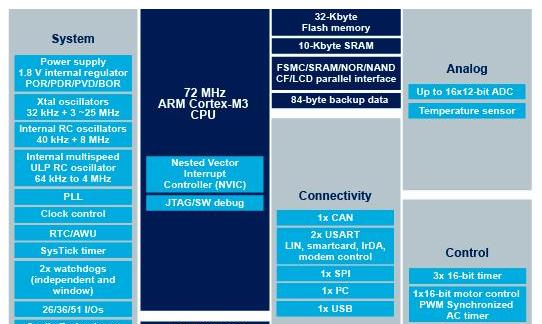
Mainstream Performance line, ARM Cortex-M3 MCU with 32 Kbytes Flash, 72 MHz CPU, motor control, USB and CAN
The STM32F103x4 and STM32F103x6 performance line family incorporates the high-performance ARM® Cortex™-M3 32-bit RISC core operating at a 72 MHz frequency, high-speed embedded memories (Flash memory up to 32 Kbytes and SRAM up to 6 Kbytes), and an extensive range of enhanced I/Os and peripherals connected to two APB buses. All devices offer two 12-bit ADCs, three general purpose 16-bit timers plus one PWM timer, as well as standard and advanced communication interfaces: up to two I2Cs and SPIs, three USARTs, an USB and a CAN.
The STM32F103xx low-density performance line family operates from a 2.0 to 3.6 V power supply. It is available in both the –40 to +85 °C temperature range and the –40 to +105 °C extended temperature range. A comprehensive set of power-saving mode allows the design of low-power applications.
The STM32F103xx low-density performance line family includes devices in four different package types: from 36 pins to 64 pins. Depending on the device chosen, different sets of peripherals are included, the description below gives an overview of the complete range of peripherals proposed in this family.
These features make the STM32F103xx low-density performance line microcontroller family suitable for a wide range of applications such as motor drives, application control, medical and handheld equipment, PC and gaming peripherals, GPS platforms, industrial applications, PLCs, inverters, printers, scanners, alarm systems, video intercoms, and HVACs.
KEY FEATURES
ARM 32-bit Cortex™-M3 CPU Core
72 MHz maximum frequency,1.25 DMIPS/MHz (Dhrystone 2.1) performance at 0 wait state memory access
Single-cycle multiplication and hardware division
Memories
16 or 32 Kbytes of Flash memory
6 or 10 Kbytes of SRAM
Clock, reset and supply management
2.0 to 3.6 V application supply and I/Os
POR, PDR, and programmable voltage detector (PVD)
4-to-16 MHz crystal oscillator
Internal 8 MHz factory-trimmed RC
Internal 40 kHz RC
PLL for CPU clock
32 kHz oscillator for RTC with calibration
Low power
Sleep, Stop and Standby modes
VBAT supply for RTC and backup registers
2 x 12-bit, 1 μs A/D converters (up to 16 channels)
Conversion range: 0 to 3.6 V
Dual-sample and hold capability
Temperature sensor
DMA
7-channel DMA controller
Peripherals supported: timers, ADC, SPIs, I2Cs and USARTs
Up to 51 fast I/O ports
26/37/51 I/Os, all mappable on 16 external interrupt vectors and almost all 5 V-tolerant
Debug mode
Serial wire debug (SWD) & JTAG interfaces
6 timers
Two 16-bit timers, each with up to 4 IC/OC/PWM or pulse counter and quadrature (incremental) encoder input
16-bit, motor control PWM timer with dead-time generation and emergency stop
2 watchdog timers (Independent and Window)
SysTick timer 24-bit downcounter
6 communication interfaces
1 x I2C interface (SMBus/PMBus)
2 × USARTs (ISO 7816 interface, LIN, IrDA capability, modem control)
1 × SPI (18 Mbit/s)
CAN interface (2.0B Active)
USB 2.0 full-speed interface
CRC calculation unit, 96-bit unique ID
Packages are ECOPACK®
Circuit Diagram
【LSM6DS33】
The LSM6DS33 is a system-in-package featuring a 3D digital accelerometer and a 3D digital gyroscope performing at 1.25 mA (up to 1.6 kHz ODR) in high-performance mode and enabling always-on low-power features for an optimal motion experience for the consumer.
The LSM6DS33 supports main OS requirements, offering real, virtual and batch sensors with 8 kbyte for dynamic data batching.
ST’s family of MEMS sensor modules leverages the robust and mature manufacturing processes already used for the production of micromachined accelerometers and gyroscopes.
The various sensing elements are manufactured using specialized micromachining processes, while the IC interfaces are developed using CMOS technology that allows the design of a dedicated circuit which is trimmed to better match the characteristics of the sensing element.
The LSM6DS33 has a full-scale acceleration range of ±2/±4/±8/±16 g and an angular rate range of ±125/±250/±500/±1000/±2000 dps.
High robustness to mechanical shock makes the LSM6DS33 the preferred choice of system designers for the creation and manufacturing of reliable products.
The LSM6DS33 is available in a plastic land grid array (LGA) package.
主要特性
Power consumption: 0.9 mA in combo normal mode and 1.25 mA in combo high-performance mode up to 1.6 kHz.
“Always-on” experience with low power consumption for both accelerometer and gyroscope
Smart FIFO up to 8 kbyte based on features set
Compliant with Android K and L
±2/±4/±8/±16 g full scale
±125/±250/±500/±1000/±2000 dps full scale
Analog supply voltage: 1.71 V to 3.6 V
Independent IOs supply (1.62 V)
Compact footprint, 3 mm x 3 mm x 0.86 mm
SPI/I2C serial interface with main processor data synchronization feature
Embedded temperature sensor
ECOPACK®, RoHS and “Green” compliant
【STP100N8F6】
N-channel 80 V, 0.008 Ohm typ., 100 A, STripFET F6 Power MOSFET in a TO-220 package
This device is an N-channel Power MOSFET developed using the STripFET™ F6 technology with a new trench gate structure. The resulting Power MOSFET exhibits very low RDS(on) in all packages.
主要特性
Very low on-resistance
Very low gate charge
High avalanche ruggedness
Low gate drive power loss
责任编辑:David
【免责声明】
1、本文内容、数据、图表等来源于网络引用或其他公开资料,版权归属原作者、原发表出处。若版权所有方对本文的引用持有异议,请联系拍明芯城(marketing@iczoom.com),本方将及时处理。
2、本文的引用仅供读者交流学习使用,不涉及商业目的。
3、本文内容仅代表作者观点,拍明芯城不对内容的准确性、可靠性或完整性提供明示或暗示的保证。读者阅读本文后做出的决定或行为,是基于自主意愿和独立判断做出的,请读者明确相关结果。
4、如需转载本方拥有版权的文章,请联系拍明芯城(marketing@iczoom.com)注明“转载原因”。未经允许私自转载拍明芯城将保留追究其法律责任的权利。
拍明芯城拥有对此声明的最终解释权。


 产品分类
产品分类




 2012- 2022 拍明芯城ICZOOM.com 版权所有 客服热线:400-693-8369 (9:00-18:00)


