基于ADI公司的ADuCM320高性能模拟微控制器开发方案
 158
158
 拍明
拍明
原标题:ADI ADuCM320高性能模拟微控制器开发方案
ADI公司的ADuCM320是采用80 MHz ARM Cortex™-M3处理器控制的高性能模拟微控制器,集成了模拟外设和数字外设以及用于代码和数据的闪存,其中的ADC提供14位1MSPS数据取样,可配置成单端或差分,DAC具有八种电压输出,主要用在10G,40G和100G光网络模块,工业控制和自动化系统,智能传感器和精密仪表以及基站系统.本文介绍了ADuCM320主要特性,框图,以及评估板EVAL-ADuCM320EBZ特性,电路图,材料清单和PCB元件布局图.
The ADuCM320 is a fully integrated single-package device that incorporates high performance analog peripherals together with digital peripherals controlled by an 80 MHz ARM Cortex™-M3 processor and integral flash for code and data.
The ADC on the ADuCM320 provides 14-bit, 1 MSPS data acquisition on up to 16 input pins that can be programmed to be single-ended or differential. Additionally, chip temperature and supply voltages can be measured. The ADC input voltage is 0 V to VREF. A sequencer is provided that allows a user selected set of ADC channels to be measured in sequence without software involvement during the sequence. The sequence can optionally auto repeat at a user-selectable rate.
Up to eight voltage DACs are provided with output ranges programmable to one of two voltage ranges. The DAC outputs have an enhanced feature of being able to retain their output voltage during a watchdog or software reset sequence. On the ADuCM320, four current output DAC sources are provided. The output currents are programmable with ranges of 0 mA to 150 mA. A low drift band gap reference and a voltage comparator complete the analog input peripheral set.
The microcontroller core is a low power ARM Cortex-M3 processor, a 32-bit RISC machine that offers up to 100 MIPS peak performance. Also integrated on chip are two 128 kB Flash/EE memory and 32 kB of SRAM. The flash comprises two separate 128 kB blocks supporting execution from one flash block and simultaneous writing/erasing of the other flash block.
The ADuCM320 operates from an on-chip oscillator or a 16 MHz external crystal and a PLL at 80 MHz. This clock can optionally be divided down to reduce current consumption. Additional low power modes can be set via software. In the normal operating mode, the ADuCM320 digital core consumes about 300 μA/MHz.
The device includes an MDIO interface capable of operating at up to 4 MHz. The capability to simultaneously execute from one flash block and write/erase the other flash block makes the ADuCM320 ideal for 40 G/100 G optical applications. User programming is eased by receiving interrupts after PHYADR, DEVADD, and end of frame and by having PHYADR and DEVADD hardware comparators. In addition, the nonerasable kernel code plus flags in user flash can provide assistance to allow user code to robustly switch between the two blocks of user flash code and data spaces as required for MDIO.
The ADuCM320 also integrates a range of on-chip peripherals that can be configured via software control as required in the application. These peripherals include one UART, two I2Cs, two SPI serial I/O communication controllers, GPIO, 32-element programmable logic array, three general-purpose timers, one wake-up timer, and one system watchdog timer. In addition, 16-bit PWMs with seven output signals are provided.
GPIO pins on the device power up in input mode with internal pull-ups on the pins of Port 0 to Port 3 and internal pull-downs on the pins of Port 4 and Port 5. In output mode, the software can choose between open-drain mode and push-pull mode. The outputs can drive at least 4 mA. The pull-ups can be disabled and enabled in software. In GPIO mode, the inputs can always be enabled to monitor the pins. The GPIO pins can also be programmed to handle digital or analog peripheral signals, in which case the pin characteristics are matched to the specific requirement.
A large support ecosystem is available for the ARM Cortex-M3 processor, which eases product development of the ADuCM320. Access is via the JTAG serial wire interface. On-chip factory firmware supports in-circuit serial download via MDIO. These features are incorporated in a low cost QuickStart development system supporting this precision analog microcontroller family.
ADuCM320主要特性:
ADC
• Multichannel, 14-bit, 1 MSPS SAR ADC
• Low drift on-chip voltage reference
DACs
• Eight voltage output DACs
• VDACs are 12-bit monotonic
• Four current output DACs
• Current DACs are 12-bit monotonic
• Low drift, on-chip 2.5 V voltage reference source
• Two buffered reference outputs
Communication
• UART
• Industry standard, 16,450 UART peripheral
• Support for DMA
• Two I2Cs
• 2-byte transmit and receive FIFOs for the master and slave
• Support for DMA
• Two SPIs
• Master or slave mode with separate 4-byte Rx and Tx FIFOs
• Rx and Tx DMA channels
• 16-bit PWM with seven output channels
• Multiple GPIO pins
Processing
• ARM Cortex-M3 processor, operating from an internal 80 MHz system clock
• Two 128 kB Flash/EE memory, 32 kB SRAM
• In-circuit download and debug via serial wire
• On-chip UART download capability
On-Chip Peripherals
• Three general-purpose timers
• Wake-up timer
• Watchdog timer
• 32-element programmable logic array (PLA)
Packages and Temperature Range
• 6 mm × 6 mm, 96-ball BGA package, −40℃ to +85℃
Tools
• Low cost development system
• Third-party compiler and emulator tool support
ADuCM320应用:
• Optical networking—10 G, 40 G, and 100 G modules
• Industrial control and automation systems
• Smart sensors, precision instrumentation
• Base station systems

图1. ADuCM320功能框图
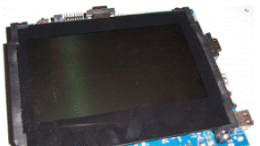
ADuCM320评估板EVAL-ADuCM320EBZ
The ADuCM320 is a dual-die stack system on-chip designed for diagnostic control on fixed wavelength laser optical module applications. It features a 16-bit (14-bit accurate) multichannel SAR ADC, an ARM® Cortex™-M3 processor, 8 voltage DACs, 4 current output DACs, and flash/EE memory packaged in a 6 mm × 6 mm 96 ball BGA package.The ADuCM320 development system allows evaluation of ADuCM320 silicon.
评估板EVAL-ADuCM320EBZ包括:
An evaluation board (EVAL-ADuCM320EBZ) that facilitates performance evaluation of the device with a minimum of external components
An Analog Devices, Inc., J-Link OB emulator (USB-SWD/UART-EMUZ)
1 USB cable
1 installation DVD

图2. 评估板EVAL-ADuCM320EBZ外形图
责任编辑:HanFeng
【免责声明】
1、本文内容、数据、图表等来源于网络引用或其他公开资料,版权归属原作者、原发表出处。若版权所有方对本文的引用持有异议,请联系拍明芯城(marketing@iczoom.com),本方将及时处理。
2、本文的引用仅供读者交流学习使用,不涉及商业目的。
3、本文内容仅代表作者观点,拍明芯城不对内容的准确性、可靠性或完整性提供明示或暗示的保证。读者阅读本文后做出的决定或行为,是基于自主意愿和独立判断做出的,请读者明确相关结果。
4、如需转载本方拥有版权的文章,请联系拍明芯城(marketing@iczoom.com)注明“转载原因”。未经允许私自转载拍明芯城将保留追究其法律责任的权利。
拍明芯城拥有对此声明的最终解释权。


 产品分类
产品分类




 2012- 2022 拍明芯城ICZOOM.com 版权所有 客服热线:400-693-8369 (9:00-18:00)


