


 产品分类
产品分类
基于Microsemi低功耗SmartFusion2 SoC FPGA开发方案
 225
225
 拍明
拍明
原标题:Microsemi低功耗SmartFusion2 SoC FPGA开发方案
Microsemi公司的SmartFusion2 SoC FPGA是低功耗FPGA器件,集成了第四代基于闪存FPGA架构,166MHz ARM Cortex-M3处理器和高性能通信接口,是业界最低功耗,最可靠和最高安全的可编逻辑解决方案.高速串行接口包括PCIe,10Gbps附加单元接口(XAUI)/XGMII)以及SerDes通信,主要用在数据安全,马达控制,系统管理,工业自动化,高速串行I/O应用,PCIe,,SGMII以及用户定义的串行接口.本文介绍了SmartFusion2 SoC FPGA主要特性,框图和芯片布局图,以及SmartFusion2 SoC FPGA评估板M2S090TS-EVAL-KIT主要特性,框图,电路图,材料清单和PCB设计图.
Microsemi SmartFusion®2 SoC FPGAs integrate a fourth-generation, flash-based FPGA fabric, an ARMCortex-M3 processor, and high-performance communications interfaces on a single chip. TheSmartFusion2 family is the industry’s lowest-power, most reliable, and highest-security programmablelogic solution.
SmartFusion2 SoC FPGAs offer up to 3.6X the gate density and up to 2X the performance of previousflash-based FPGA families, and also include multiple memory blocks and multiply-accumulate blocks forDSP processing. The 166-MHz ARM Cortex-M3 processor is enhanced with an embedded tracemacrocell (ETM), a memory protection unit (MPU), an 8-KB instruction cache, and additional peripherals,including controller area network (CAN), gigabit Ethernet, and a high-speed universal serial bus (USB).
High-speed serial interfaces include PCI Express (PCIe), 10-Gbps Attachment Unit Interface(XAUI)/XGMII extended sublayer (XGXS), plus native serialization/deserialization (SerDes)communication. The DDR2/DDR3 memory controllers available in the devices provide high-speedmemory interfaces.
SmartFusion2 SoC FPGA主要特性:
The following sections list the features of SmartFusion2 SoC FPGAs.
Reliability
• Single event upset (SEU)-immune
• Zero FIT FPGA configuration cells
• Junction temperature
• 125 °C—military temperature
• 100 °C—industrial temperature
• 85 °C—commercial temperature
• 125 °C—automotive
• Single error correct double error detect (SECDED) protection on the following:
• Ethernet buffers
• CAN message buffers
• Cortex-M3 embedded scratch pad memory (eSRAMs)
• USB buffers
• PCIe buffer
• DDR memory controllers with optional SECDED modes
• Buffers implemented with SEU resistant latches on the following:
• DDR bridges (MSS, MDDR, and FDDR)
• Instruction cache
• MMUART FIFOs
• SPI FIFOs
• NVM integrity check at power-up and on demand
• No external configuration memory required—instant-on, retains configuration when powered off
Security
• Design security features (available on all devices)
• Intellectual property (IP) protection through unique security features and use models new to thePLD industry
• Built-in CRI DPA pass-through license from Rambus Cryptography Research
• Encrypted user key and bitstream loading, enabling programming in less-trusted locations
• Supply-chain assurance device certificate
• Enhanced anti-tamper features
• Zeroization
• Data security features
• Non-deterministic random bit generator (NRBG)
• User cryptographic services (AES-256, SHA-256, and elliptical curve cryptographic (ECC)engine)
• User physically unclonable function (PUF) key enrollment and regeneration
• CRI pass-through DPA patent portfolio license
• Hardware firewalls protecting microcontroller subsystem (MSS) memories
Low Power
• Low static and dynamic power
• Flash*Freeze mode for fabric
• Power as low as 13 mW/Gbps per lane for SerDes devices
• Up to 50% lower total power than competing SoC devices
High Performance
• Efficient 4-input look-up tables (LUTs) with carry chains for high performance and low power
• Up to 236 blocks of dual-port 18-Kbit SRAM (LSRAM) with 400 MHz synchronous performance (512
× 36, 512 × 32, 1 Kb × 18, 1 Kb × 16, 2 kbit × 9, 2 Kb × 8, 4 Kb × 4, 8 Kb × 2, or 16 Kb × 1)
• Up to 240 blocks of three-port 1-Kb SRAM with two read ports and one write port (micro SRAM)
• High-performance DSP signal processing
• Up to 240 fast mathblocks with 18 × 18 signed multiplication, 17 × 17 unsigned multiplicationand 44-bit accumulator
Microcontroller Subsystem
• Hard 166-MHz 32-Bit ARM Cortex-M3 processor
• 1.25 DMIPS/MHz
• 8 Kbyte instruction cache
• Embedded trace macrocell (ETM)
• Memory protection unit (MPU)
• Single cycle multiplication, hardware divide
• JTAG debug (4 wires), serial wire debug (SWD, 2 wires), and serial wire viewer (SWV)
interfaces
• 64 KB embedded SRAM (eSRAM)
• Up to 512 KB embedded nonvolatile memory (eNVM)
• Triple-speed Ethernet (TSE) 10/100/1000 Mbps MAC
• USB 2.0 high speed on-the-go (OTG) controller with ULPI interface
• 2.0B-compliant CAN controller, conforms to ISO11898-1, 32 transmit and 32 receive buffers
• Two SPI ports, two I2C ports, and multi-mode UARTs (MMUART) peripherals
• Hardware-based watchdog timer
• One general-purpose 64-bit (or two 32-bit) timer(s)
• Real-time calendar/counter (RTC)
• DDR bridge (4-port data R/W buffering bridge to DDR memory) with 64-bit AXI interface
• Non-blocking, multi-layer AHB bus matrix allowing multi-master scheme supporting 10 masters and7 slaves
• Two AHB-Lite/APB3 interfaces to FPGA fabric (master/slave-capable)
• Two DMA controllers to offload data transactions from the Cortex-M3 processor
• 8-channel peripheral DMA (PDMA) for data transfer between MSS peripherals and memory
• High-performance DMA (HPDMA) for data transfer between eSRAM and DDR memories
Clocking Resources
• Clock sources
• Up to two high precision 32 KHz to 20 MHz main crystal oscillator
• 1-MHz embedded RC oscillator
• 50-MHz embedded RC oscillator
• Up to eight clock conditioning circuits (CCCs) with up to eight integrated analog PLLs
• Output clock with eight output phases and 45° phase difference (multiply/divide and delaycapabilities)
• Frequency: 1 MHz to 200 MHz input, 20 MHz to 400 MHz output
High-Speed Serial Interfaces
• Up to 16 SerDes lanes, each supporting:
• XGXS/XAUI extension (to implement a 10-Gbps (XGMII) Ethernet PHY interface)
• Native EPCS SerDes interface that facilitates implementation of serial rapidIO (SRIO) in fabricor an SGMII interface to the Ethernet MAC in MSS
• PCI express (PCIe) endpoint controller
• ×1, ×2, and ×4 lane PCI express core
• Maximum payload size of up to 256 bytes
• 64-bit/32-bit AXI interface and 64-Bit/32-Bit AHB master and slave interfaces to the applicationlayer
High-Speed Memory Interfaces
• Up to two high-speed DDRx memory controllers
• MSS DDR (MDDR) and fabric DDR (FDDR) controllers
• Supports LPDDR/DDR2/DDR3
• Maximum 333 MHz DDR clock rate
• SECDED enable/disable feature
• Supports various DRAM bus width modes, ×8, ×9, ×16, ×18, ×32, ×36
• Supports command reordering to optimize memory efficiency
• Supports data reordering, returning critical word first for each command
• SDRAM support through the SMC_FIC and additional soft SDRAM memory controller
Operating Voltage and I/Os
• 1.2 V core voltage
• Multi-standard user I/Os (MSIO/MSIOD)
• LVTTL/LVCMOS 3.3 V (MSIO Only)
• LVCMOS 1.2 V, 1.5 V, 1.8 V, 2.5 V
• DDR (SSTL2_1, SSTL2_2)
• LVDS, MLVDS, Mini-LVDS, RSDS differential standards
• PCI
• LVPECL (receiver only)
• DDR I/Os (DDRIO)
• DDR2, DDR3, LPDDR, SSTL2, SSTL18, HSTL
• LVCMOS 1.2 V, 1.5 V, 1.8 V, 2.5 V
• Market-leading number of user I/Os with 5G SerDes
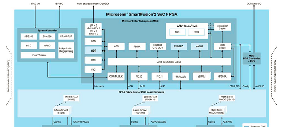
图1.SmartFusion2 SoC FPGA框图
SmartFusion2 flash-based fabric has zero FIT configuration rate due to its SEU immunity, which is criticalin reliability applications. The flash fabric also has the advantage that no external configuration memoryis required, making the device instant-on; it retains configuration when powered off. To complement thisunique FPGA capability, SmartFusion2 devices add reliability to many other aspects of the device. Singleerror correct double error detect (SECDED) protection is implemented on the Cortex-M3 embeddedscratch pad memory, Ethernet, CAN, and USB buffers, and is optional on the DDR memory controllers.
This means that if a one-bit error is detected, the error is corrected automatically. If errors of more thanone bit are detected, they are not corrected. SECDED error signals are brought to the FPGA fabric toallow the user to monitor the status of these protected internal memories. Other areas of the architectureare implemented with latches, which are more resistant to SEUs. Therefore, no correction is needed inDDR bridges (MSS, MDDR, and FDDR), instruction cache and MMUART, SPI, and PCIe FIFOs.

图2.SmartFusion2 SoC FPGA芯片布局图
SmartFusion2 SoC FPGA评估板M2S090TS-EVAL-KIT
The RoHS-compliant SmartFusion®2 SoC FPGA Security Evaluation Kit (M2S090TS-EVAL-KIT) enablesyou to develop the following types of applications:
• Data security
• Motor control
• System management
• Industrial automation
• High-speed serial I/O applications:
• Peripheral component interconnect express (PCIe)
• Serial-gigabit media independent interface (SGMII)
• User-customizable serial interfaces
评估板M2S090TS-EVAL-KIT包括:

评估板M2S090TS-EVAL-KIT主要特性:
The M2S090TS-EVAL-KIT offers a full-featured evaluation board for SmartFusion2 SoC FPGAs. Theboard integrates the following features on a single chip.
• Reliable flash-based FPGA fabric
• 166 MHz ARM Cortex-M3 processor
• Advanced security processing accelerators
• Digital signal processing (DSP) blocks
• Static random-access memory (SRAM)
• Embedded non-volatile memory (eNVM)
• High-performance communication interfaces
The SmartFusion2 Security Evaluation Board has several standard interfaces, including.
• An RJ45 connector for 10/100/1000 Mbps Ethernet
• A full-duplex serializer/deserializer (SerDes) lane connected through sub-miniature version A (SMA)connectors
• A 64-bit GPIO header
• Various connectors for serial peripheral interface (SPI) support
The SmartFusion2 memory management system supports 512 Mb on-board low-power double data rate(LPDDR) SDRAM memory and 64 Mb SPI flash memory. The SerDes block can either be accessedusing the PCIe edge connector or using high-speed SMA connectors.

图.评估板M2S090TS-EVAL-KIT外形图
评估板M2S090TS-EVAL-KIT材料清单见设计文件
![]() Microsemi_SmartFusion2_Security_Evaluation_Kit_User_Guide_UG0594.pdf.pdf
Microsemi_SmartFusion2_Security_Evaluation_Kit_User_Guide_UG0594.pdf.pdf
![]() m2s_m2gl_ds0120_mil_v4.pdf.pdf
m2s_m2gl_ds0120_mil_v4.pdf.pdf
责任编辑:Davia
【免责声明】
1、本文内容、数据、图表等来源于网络引用或其他公开资料,版权归属原作者、原发表出处。若版权所有方对本文的引用持有异议,请联系拍明芯城(marketing@iczoom.com),本方将及时处理。
2、本文的引用仅供读者交流学习使用,不涉及商业目的。
3、本文内容仅代表作者观点,拍明芯城不对内容的准确性、可靠性或完整性提供明示或暗示的保证。读者阅读本文后做出的决定或行为,是基于自主意愿和独立判断做出的,请读者明确相关结果。
4、如需转载本方拥有版权的文章,请联系拍明芯城(marketing@iczoom.com)注明“转载原因”。未经允许私自转载拍明芯城将保留追究其法律责任的权利。
拍明芯城拥有对此声明的最终解释权。
相关资讯
:
基于MC33771主控芯片的新能源锂电池管理系统解决方案

AMIC110 32位Sitara ARM MCU开发方案

基于AMIC110多协议可编程工业通信处理器的32位Sitara ARM MCU开发方案

基于展讯SC9820超低成本LTE芯片平台的儿童智能手表解决方案

基于TI公司的AM437x双照相机参考设计

基于MTK6580芯片的W2智能手表解决方案


 2012- 2022 拍明芯城ICZOOM.com 版权所有 客服热线:400-693-8369 (9:00-18:00)


