基于ST公司的STM32F334C8 500W全数字电源解决方案
 130
130
 拍明
拍明
原标题:ST STM32F334C8 500W全数字电源解决方案
ST公司的STM32F334x4/6/8系列产品是高性能32位ARM Cortex-M4 MCU,工作频率高达72MHz,并嵌入了浮点单元(FPU),集成了高速嵌入存储器(多达64KB闪存和多达12KB SRAM)以及连接于两条APB总线的各种增强I/O和外设.本文介绍了STM32F334x4/6/8系列产品,框图,以及采用STM32F334C8 MCU的500W 全数字AC/DC电源STEVAL-ISA147V2主要指标,框图,电路图,材料清单和PCB元件布局和走线图.
The STM32F334x4/6/8 family is based on the high-performance ARMR32-bit CortexR-M4 RISC core operating at a frequency of up to 72 MHz, and embedding a floating point unit (FPU). The STM32F334x4/6/8 family incorporates high-speed embedded memories (up to 64 Kbytes of Flash memory, up to 12 Kbytes of SRAM), and an extensive range of enhanced I/Os and peripherals connected to two APB buses.
The STM32F334x4/6/8 devices offer a High resolution timer, two fast 12-bit ADCs (5 Msps), up to three ultra-fast comparators, an operational amplifier, three DAC channels, a lowpower RTC, one high-resolution timer, one general-purpose 32-bit timer, one timer dedicated to motor control, and four general-purpose 16-bit timers. They also feature standard and advanced communication interfaces: one I2C, one SPI, up to three USARTs and one CAN.
The STM32F334x4/6/8 family operates in the –40 to +85 °C and –40 to +105 °C temperature ranges from a 2.0 to 3.6 V power supply. A comprehensive set of power-saving mode allows the design of low-power applications.
The STM32F334x4/6/8 family offers devices in 32, 48 and 64-pin packages.
STM32F334C8主要特性:
• Core: ARMR-32-bit-CortexR-M4 CPU with FPU (72 MHz max), single-cycle multiplication and HW division, and DSP instruction
• Memories
– Up to 64 KB of Flash memory
– Up to 12 KB of SRAM with HW parity check
– Routine booster: 4 KB of SRAM on instruction and data bus with HW parity check (CCM)
• CRC calculation unit
• Reset and supply management
– VDD,VDDA voltage range: 2.0 to 3.6 V
– Power-on/Power-down reset (POR/PDR)
– Programmable voltage detector (PVD)
– Low-power modes: Sleep,Stop,Standby
– VBAT supply for RTC and backup registers
• Clock management
– 4 to 32 MHz crystal oscillator
– 32 kHz oscillator for RTC with calibration
– Internal 8 MHz RC (up to 64 MHz with PLL option)
– Internal 40 kHz oscillator
• Up to 51fast I/O ports, all mappable on external interrupt vectors, several 5 V-tolerant
• 7-channel DMA controller
• Up to two ADC 0.20 μs (up to 21 channels) with selectable resolution of 12/10/8/6 bits, 0 to
3.6 V conversion range, singleended/differential mode, separate analog supply from 2.0 to 3.6 V
• Temperature sensor
• Up to three 12-bit DAC channels with analog supply from 2.4 V to 3.6 V
• Three ultra-fast rail-to-rail analog comparators with analog supply from 2 V to 3.6 V
• One operational amplifiers that can be used in PGA mode, all terminals accessible with analog supply from 2.4 to 3.6 V
• Up to 18 capacitive sensing channels supporting touchkeys, linear and rotary touch sensors
• Up to 12 timers
– HRTIM: 6 x16-bit counters, 217 ps resolution, 10 PWM, 5 fault inputs, 10 ext event input, 1 synchro. input,1 synchro. out
– One 32-bit timer and one 16-bit timer with up to 4 IC/OC/PWM or pulse counter and quadrature (incremental) encoder input
– One 16-bit 6-channel advanced-control timer, with up to 6 PWM channels, deadtime generation and emergency stop
– One 16-bit timer with 2 IC/OCs, 1 OCN/PWM, deadtime generation, emergency stop
– Two 16-bit timers with IC/OC/OCN/PWM, deadtime generation and emergency stop
– Two watchdog timers (independent, window)
– SysTick timer: 24-bit downcounter
– Up to two 16-bit basic timers to drive the DAC
• Calendar RTC with alarm, periodic wakeup from Stop
• Communication interfaces
– CAN interface (2.0 B Active)
– One I2C with 20 mA current sink to support Fast mode plus, SMBus/PMBus
– Up to 3 USARTs, one with ISO/IEC 7816 interface, LIN, IrDA, modem control
– One SPI
• Debug mode: serial wire debug (SWD), JTAG
• 96-bit unique ID
• All packages ECOPACKR2

图1. STM32F334x4/6/8框图
采用STM32F334C8 MCU的500W 全数字AC/DC电源STEVAL-ISA147V2
The STEVAL-ISV147V2 is a digital switch mode AC-DC converter consisting of two power stages: an input semi-bridgeless power factor corrector (SBPFC) controlled by an STM32F051K8, and a regulation stage implemented with a LLC half bridge with synchronous rectification (SR), controlled by an STM32F334C8 microcontroller. This 500 W AC-DC converter uses the so-called bridgeless PFC topology which has the advantage of lower conduction losses and higher efficiency by eliminating the need for a diode rectifier stage. This choice also allows reduction of component count compared to a standard PFC. The input stage is typically controlled using an outer voltage loop for bus voltage regulation and an inner control loop to shape the current according to a sinusoidal waveform. The outer loop adjusts the current reference in order to maintain a regulated bus voltage independent of the load or input voltage variations. The output isolation and regulation stage is implemented using a half-bridge LLC topology operating with constant duty cycle and variable frequency control.
The DC-DC stage performs voltage step-down using an HF transformer with a primary to secondary turns ratio chosen to maintain good efficiency and regulation over the entire operating range. The transformer is supplied with a square wave voltage generated by the primary side active switches. On the secondary side this voltage waveform is rectified and then smoothed by the output filter, while on the primary side switching losses are reduced thanks to zero voltage switching (ZVS). On the secondary side, synchronous rectification (SR) is used to ensure low conduction losses. The overall effect of these design choices is high system efficiency, in line with the stringent requirements of the power supply industry.
The system is controlled by two microcontrollers from the STM32 product family. On the primary side, an STM32F051K8 controls the bridgeless PFC by sampling the current of the two MOSFETs, the input AC voltage and the output bus voltage. Two control signals, PWM1 and PWM2, are then generated to drive two power switches. On the secondary side, an STM32F334C8 microcontroller samples the output voltage and adjusts the frequency of the LLC bridge control signals to ensure stable operation throughout the overall load range. In addition, two ADC channels are used to sample the rising and falling edges of the drain-to-source voltage of the SR MOSFETs. The two microcontrollers exchange information about the status of the input and output power stage via bidirectional serial communication.
Both the power stage and control stage are supplied by an offline flyback circuit which provides a suitable regulated voltage to the microcontrollers, the gate drive ICs and signal conditioning circuits
500W 全数字AC/DC电源STEVAL-ISA147V2主要特性:
Input AC voltage: 90 V to 264 V
Input AC frequency: 45 Hz to 65 Hz
Nominal power: 500 W
Bridgeless PFC stage
DC-DC stage: resonant LLC with synchronous rectification
Peak efficiency: 93.2%
PFC switching frequency: 60 kHz
DC-DC switching frequency: 70 kHz to 130 kHz
HF transformer isolation voltage: 4 kV
Cooling: natural convection up to 300 W, forced cooling above 300 W
Input short-circuit protection: 10 A fuse
PFC control: managed by STM32F051K8
LLC control: managed by STM32F334C8
RoHS compliant

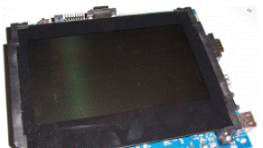
图2.500W数字电源板STEVAL-ISA147V2外形图

图3.500W数字电源板STEVAL-ISA147V2框图
500W数字电源板STEVAL-ISA147V2主要技术指标:

500W数字电源板STEVAL-ISA147V2材料清单:


责任编辑:HanFeng
【免责声明】
1、本文内容、数据、图表等来源于网络引用或其他公开资料,版权归属原作者、原发表出处。若版权所有方对本文的引用持有异议,请联系拍明芯城(marketing@iczoom.com),本方将及时处理。
2、本文的引用仅供读者交流学习使用,不涉及商业目的。
3、本文内容仅代表作者观点,拍明芯城不对内容的准确性、可靠性或完整性提供明示或暗示的保证。读者阅读本文后做出的决定或行为,是基于自主意愿和独立判断做出的,请读者明确相关结果。
4、如需转载本方拥有版权的文章,请联系拍明芯城(marketing@iczoom.com)注明“转载原因”。未经允许私自转载拍明芯城将保留追究其法律责任的权利。
拍明芯城拥有对此声明的最终解释权。


 产品分类
产品分类




 2012- 2022 拍明芯城ICZOOM.com 版权所有 客服热线:400-693-8369 (9:00-18:00)


