基于NXP公司的LPC546XX系列32位ARM MCU嵌入应用开发方案
 384
384
 拍明
拍明
原标题:NXP LPC546XX系列32位ARM MCU嵌入应用开发方案
LPC546xx MCU系列集成了高效的220 MHz Arm® Cortex®-M4内核、多种高速连接选项、高级定时器和模拟功能。DSP功能使LPC546xx MCU器件可以支持数据密集型应用的复杂算法。该系列可灵活提供高达512 KB闪存和外部存储器接口,能够适应变化需求。闪存选项支持灵活的内部和外部大型存储器配置。借助LPC54000系列的内置兼容性,LPC546xx MCU系列能够提供一个无缝的迁移路径来提高处理性能,并增加其他先进外设的灵活性。
nxp公司的LPC546XX系列是基于32位ARM Cortex-M4核的MCU,具有系统增强功能如低功耗,增强的调试特性,集成了高等级的支持区块.器件采用3级流水线,具有单独本地指令和数据总线以及用于外设的第三总线的哈佛架构,集成了多达512KB 闪存,200KB SRAM,高速USB device/host + PHY,全速USBdevice/host,以太网AVB, LCD; EMC; SPIFI; CAN FD,SDIO, SHA,12-bit 5 MSPS ADC; DMIC子系统,工作频率高达220MHz,主要用在嵌入式应用领域.本文介绍了LPC546XX系列主要特性和优势,框图,以及LPCXpresso546xx系列评估板主要特性和主要特性布局图,框图,电路图和材料清单.
The LPC546xx is a family of ARM Cortex-M4 based microcontrollers for embedded applications featuring a rich peripheral set with very low power consumption and enhanced debug features.
The ARM Cortex-M4 is a 32-bit core that offers system enhancements such as low power consumption, enhanced debug features, and a high level of support block integration. The ARM Cortex-M4 CPU incorporates a 3-stage pipeline, uses a Harvard architecture with separate local instruction and data buses as well as a third bus for peripherals, and includes an internal prefetch unit that supports speculative branching. The ARM Cortex-M4 supports single-cycle digital signal processing and SIMD instructions. A hardware floating-point processor is integrated into the core.
The LPC546xx family includes up to 512 KB of flash, 200 KB of on-chip SRAM, up to 16 kB of EEPROM memory, a quad SPI Flash Interface (SPIFI) for expanding program memory, one high-speed and one full-speed USB host and device controller, Ethernet AVB, LCD controller, Smart Card Interfaces, SD/MMC, CAN FD, an External Memory Controller (EMC), a DMIC subsystem with PDM microphone interface and I2S, five general-purpose timers, SCTimer/PWM, RTC/alarm timer, Multi-Rate Timer (MRT), a Windowed Watchdog Timer (WWDT), ten flexible serial communication peripherals(USART, SPI, I2S, I2C interface), Secure Hash Algorithm (SHA), 12-bit 5.0 Msamples/sec ADC, and a temperature sensor.
特性
Arm Cortex-M4内核(版本r0p1)
片上存储器
最高512 KB片上可编程闪存,带闪存加速器和256字节页面擦除和写入功能。
最高200 KB总SRAM,包含160 KB连续主SRAM和I&D总线上额外的32 KB SRAM。8 KB SRAM块用于USB流量。
16 KB EEPROM。
支持ROM API
闪存在应用编程(IAP)和在系统编程(ISP)。
基于ROM的USB驱动程序(HID、CDC、MSC和DFU)。通过USB进行闪存更新。
通过闪存、USART、SPI和I2C中的有效用户代码引导。
传统引导、单双图像引导。
面向可编程的OTP存储器的OTP API。
随机数生成器(RNG) API。
Flexcomm接口包含10个串行外设。每个Flexcomm接口可通过软件选择作为USART、SPI或I2C接口。两个Flexcomm接口也包含一个I2S接口。每个Flexcomm接口包含一个FIFO,支持该Flexcomm接口所支持的USART、SPI和I2S。每个Flexcomm接口具有多种时钟选项,包含一个共享的分数波特率生成器。
I2C总线接口,支持Fast-Mode和Fast-Mode Plus,数据传输率高达1 Mbit/S,具有多种地址识别和监控模式。两组真正的I2C焊盘,支持从设备高速模式(3.4 Mbit/S)
两个ISO 7816智能卡接口,支持DMA。
USB 2.0高速主机/器件控制器,带片上高速PHY。
USB 2.0全速主机/器件控制器,带片上PHY和专用DMA控制器,在器件模式中支持无晶振工作。
带XIP特性的SPIFI,使用最多4条数据线来接入片外SPI/DSPI/QSPI闪存,速率比标准SPI或SSP接口高很多。
以太网MAC带MII/RMIIRMII接口、音视频桥接(AVB)支持以及专用DMA控制器。
两个CAN FD模块,带专用DMA控制器。
数字外设
DMA控制器,具有30个通道和24个可编程触发器,能够访问所有存储器和支持DMA的外设。
LCD控制器,同时支持超扭曲向列液晶(STN)和薄膜晶体管(TFT)显示。它有一个专用的DMA控制器,可选的显示分辨率(最高1024 x 768像素),支持24位真彩模式。
外部存储控制器(EMC)支持异步静态存储器设备,例如RAM、ROM、闪存、以及动态存储器,如单数据速率SDRAM,其SDRAM时钟最高达100 MHz。
安全的数字输入输出(SD/MMC和SDIO)卡接口,支持DMA
CRC引擎模块可使用支持DMA的3个标准多项式中的一个计算所提供数据的CRC。
最多171个通用输入/输出(GPIO)引脚。
通用IO寄存器位于AHB上,以支持快速存取。DMA支持通用IO端口。
最多8个通用IO可选为引脚中断(PINT),由上升沿、下降沿或两种输入沿触发。
两组通用IO中断(GINT)支持基于输入状态逻辑(AND/OR)组合的中断
CRC引擎。
模拟外设
12位ADC,具有12个输入通道以及多个内部和外部触发器输入,采样速率高达5.0 M采样/秒。该ADC支持两个独立的转换序列。
连接至ADC的集成式温度传感器。
定时器
5个32位通用定时器/计数器,其中4个支持最多4个采集输入和4个比较输出、PWM模式和外部计数输入。可选择特定的定时器事件,以生成DMA请求。第5个定时器没有外部引脚连接,可用于内部定时操作。
一个SSCTimer/PWM,具有8个输入和10个输出函数(包括采集和匹配)。输入和输出可引至或引自外部引脚,内部引至或引自所选外设。在内部,SSCTimer/PWM支持16个采集/匹配,16个事件和10个状态。
32位实时时钟(RTC),以1 S分辨率在始终开启的电源域内运行。RTC中的定时器可用于唤醒所有低功耗模式(包括深度节电模式),具有1 ms分辨率。
多通道多速率24位定时器(MRT),用于在最多4种可编程固定速率下重复生成中断。
窗口化看门狗定时器(WWDT)。
重复中断定时器(RIT),用于调试时间戳和通用用途
安全的外设
增强的代码读取保护(eCRP)用于保护用户代码。
时钟生成
12 MHz内部自激振荡器(FRO)。该振荡器提供可选择的48 MHz或96 MHz输出,以及一个可用作系统时钟的12 MHz输出(从所选的较高频率中分离)。FRO在整个电压和温度范围内调校为±1 %精确度。
高达25 MHz的外部时钟输入时钟频率。
工作频率范围为1 MHz至25 MHz的晶体振荡器。
看门狗振荡器(WDTOSC),频率范围为200 kHz至1.5 MHz。
32.768 kHz低功耗RTC振荡器。
系统PLL允许CPU运行最高CPU速度,可通过主振荡器、内部FRO、看门狗振荡器或32.768 KHz时钟振荡器运行。
两个额外的PLL,用于USB时钟和音频子系统。
独立的时钟,用于SPIFI接口、ADC、USB和音频系统。
带除法器的时钟输出函数。
用于测量片上和片下时钟信号频率的频率测量单元。
更多信息
DMIC子系统包含一个双通道PDM麦克风接口、灵活抽取器、16条FIFO、可选DC锁定、硬件语音活动检测,以及将经过处理的输出数据流式传输至I2S的选项。
单电源1.71 V至3.6 V。
上电复位(POR)。
带独立阈值的掉电检测(BOD),用于中断和强制复位。
支持JTAG边界扫描。
128位唯一器件识别序列号。
工作温度范围为-40 °C至+105 °C。
LPC546XX系列主要特性和优势:
ARM Cortex-M4 core (version r0p1):
ARM Cortex-M4 processor, running at a frequency of up to 220 MHz.
The LPC5460x/61x devices operate at CPU frequencies of up to 180 MHz. The LPC54628 device operates at CPU frequencies of up to 220 MHz.
Floating Point Unit (FPU) and Memory Protection Unit (MPU).
ARM Cortex-M4 built-in Nested Vectored Interrupt Controller (NVIC).
Non-maskable Interrupt (NMI) input with a selection of sources.
Serial Wire Debug (SWD) with six instruction breakpoints, two literal comparators,and four watch points.Includes Serial Wire Output and ETM Trace for enhanceddebug capabilities, and a debug timestamp counter.
System tick timer.
On-chip memory:
Up to 512 KB on-chip flash program memory with flash accelerator and 256 bytepage erase and write.
Up to 200 KB total SRAM consisting of 160 KB contiguous main SRAM and an additional 32 KB SRAM on the I&D buses. 8 KB of SRAM bank intended for USBtraffic.
16 KB of EEPROM.
ROM API support:
Flash In-Application Programming (IAP) and In-System Programming (ISP).
ROM-based USB drivers (HID, CDC, MSC, and DFU). Flash updates via USB.
Booting from valid user code in flash, USART, SPI, and I2C.
Legacy, Single, and Dual image boot.
OTP API for programming OTP memory.
Random Number Generator (RNG) API.
Serial interfaces:
Flexcomm Interface contains up to ten serial peripherals. Each Flexcomm Interface can be selected by software to be a USART, SPI, or I2C interface. Two Flexcomm Interfaces also include an I2S interface. Each Flexcomm Interface includes a FIFO that supports USART, SPI, and I2S if supported by that Flexcomm Interface. A variety of clocking options are available to each Flexcomm Interface and include a shared fractional baud-rate generator.
I2C-bus interfaces support Fast-mode and Fast-mode Plus with data rates of up to 1Mbit/s and with multiple address recognition and monitor mode. Two sets of trueI2C pads also support High Speed Mode (3.4 Mbit/s) as a slave.
Two ISO 7816 Smart Card Interfaces with DMA support.
USB 2.0 high-speed host/device controller with on-chip high-speed PHY.
USB 2.0 full-speed host/device controller with on-chip PHY and dedicated DMA controller supporting crystal-less operation in device mode.
SPIFI with XIP feature uses up to four data lines to access off-chip SPI/DSPI/QSPI
flash memory at a much higher rate than standard SPI or SSP interfaces.
Ethernet MAC with MII/RMII interface with Audio Video Bridging (AVB) support and
dedicated DMA controller.
Two CAN FD modules with dedicated DMA controller.
Digital peripherals:
DMA controller with 30 channels and up to 24 programmable triggers, able toaccess all memories and DMA-capable peripherals.
LCD Controller supporting both Super-Twisted Nematic (STN) and Thin-Film Transistor (TFT) displays. It has a dedicated DMA controller, selectable display resolution (up to 1024 x 768 pixels), and supports up to 24-bit true-color mode.
External Memory Controller (EMC) provides support for asynchronous static memory devices such as RAM, ROM and flash, in addition to dynamic memories such as single data rate SDRAM with an SDRAM clock of up to 100 MHz. EMC bus width (bit) on LQFP100 and TFBGA100 packages supports up to 8/16 data line wide static memory, in addition to dynamic memories, such as, SDRAM (2 banks only) with an SDRAM clock of up to 100 MHz.
Secured digital input/output (SD/MMC and SDIO) card interface with DMA support.
CRC engine block can calculate a CRC on supplied data using one of three
standard polynomials with DMA support.
Up to 171 General-Purpose Input/Output (GPIO) pins.
GPIO registers are located on the AHB for fast access. The DMA supports GPIO ports.
Up to eight GPIOs can be selected as Pin Interrupts (PINT), triggered by rising,falling or both input edges.
Two GPIO Grouped Interrupts (GINT) enable an interrupt based on a logical(AND/OR) combination of input states.
CRC engine.
Analog peripherals:
12-bit ADC with 12 input channels and with multiple internal and external trigger inputs and sample rates of up to 5.0 MSamples/sec. The ADC supports two independent conversion sequences.
Integrated temperature sensor connected to the ADC.
DMIC subsystem including a dual-channel PDM microphone interface, flexible decimators, 16 entry FIFOs, optional DC locking, hardware voice activity detection,and the option to stream the processed output data to I2S.
Timers:
Five 32-bit general purpose timers/counters, four of which support up to four capture inputs and four compare outputs, PWM mode, and external count input.
Specific timer events can be selected to generate DMA requests. The fifth timer does not have external pin connections and may be used for internal timing operations.
SCTimer/PWM with 8 input and 10 output functions (including capture and match). Inputs and outputs can be routed to/from external pins and internally to or from selected peripherals. Internally, the SCTimer/PWM supports 10 match/captures, 10 events, and 10 states.
32-bit Real-time clock (RTC) with 1 s resolution running in the always-on power domain. A timer in the RTC can be used for wake-up from all low power modes including deep power-down, with 1 ms resolution.
Multiple-channel multi-rate 24-bit timer (MRT) for repetitive interrupt generation at
up to four programmable, fixed rates.
Windowed Watchdog Timer (WWDT).
Repetitive Interrupt Timer (RIT) for debug time stamping and for general purposeuse.
Security features:
enhanced Code Read Protection (eCRP) to protect user code.
OTP memory for ECRP settings, and user application specific data.
Secure Hash Algorithm (SHA1/SHA2) module with dedicated DMA controller.
Clock generation:
12 MHz internal Free Running Oscillator (FRO). This oscillator provides a selectable 48 MHz or 96 MHz output, and a 12 MHz output (divided down from the selected higher frequency) that can be used as a system clock. The FRO is trimmed to +/- 1 % accuracy over the entire voltage and temperature range.
External clock input for clock frequencies of up to 25 MHz.
Crystal oscillator with an operating range of 1 MHz to 25 MHz.
Watchdog Oscillator (WDTOSC) with a frequency range of 6 kHz to 1.5 MHz.
32.768 kHz low-power RTC oscillator.
System PLL allows CPU operation up to the maximum CPU rate and can run from the main oscillator, the internal FRO, the watchdog oscillator or the 32.768 KHz RTC oscillator.
Two additional PLLs for USB clock and audio subsystem.
Independent clocks for the SPIFI interface, ADC, USBs, and the audio subsystem.
Clock output function with divider.
Frequency measurement unit for measuring the frequency of any on-chip oroff-chip clock signal.
Power control:
Programmable PMU (Power Management Unit) to minimize power consumptionand to match requirements at different performance levels.
Reduced power modes: sleep, deep-sleep, and deep power-down.
Wake-up from deep-sleep modes due to activity on the USART, SPI, and I2C
peripherals when operating as slaves.
Ultra-low power Micro-tick Timer, running from the Watchdog oscillator that can be used to wake up the device from low power modes.
Power-On Reset (POR).
Brown-Out Detect (BOD) with separate thresholds for interrupt and forced reset.
Single power supply 1.71 V to 3.6 V.
Power-On Reset (POR).
Brown-Out Detect (BOD) with separate thresholds for interrupt and forced reset.
JTAG boundary scan supported.
128 bit unique device serial number for identification.
Operating temperature range - 40 °C to +105 °C.
Available in TFBGA180, TFBGA100, LQFP208, and LQFP100 packages.
LPC546xx MCU产品
LPC5460x:具有HMI和连接选项的高效节能MCU
LPC5461x:增加CAN-FD功能
目标应用
楼宇控制和自动化
诊断设备
多节点/多协议通信集线器
HMI/GUI应用
数据收集器、车载信息娱乐系统/导航
远程信息处理/车队管理
LPCXpresso54608/54618/54628评估板
The LPCXpresso™ family of boards provides a powerful and flexible development system for NXP ’ s LPC Cortex®-M family of MCUs. They can be used with a wide range of development tools, including NXP’s MCUXpresso IDE. The LPCXpresso54608 (OM13092), LPCXpresso54618 (board provided as part of the OM13094 CAN-FD Kit) and LPCXpresso54628 (OM13098) share the same design and have been developed by NXP to enable evaluation of and prototyping with the LPC546xx family of MCUs. There is no functional difference between these boards except the (1) functionality of the LPC546xx device installed, and (2) that the LPC54618 board included in the OM13094 does not include the LCD panel. All boards use a BGA180 package.
Note that the LPCXpresso54628 board features an LPC54628 device which has a superset of functionality compared to the LPC54608 and LPC54618. This means code written for the LPC54608 and LPC54618 can run unchanged on the LPC54628. The LPC54628 is capable of running at up to 220MHz, but requires a different power library (from the MCUXpresso SDK) than the other devices in order to run at this clock speed. Initially this library will be available as a separate download until it is fully integrated into the SDK in Q4 2017.
The schematics show that the board was designed for either 1.8 V or 3.3 V build configurations, but all production boards are built in the 3.3 V configuration.
LPCXpresso54608/54618/54628评估板主要特性:
• On-board, high-speed USB based, Link2 Debug Probe with CMSIS-DAP and SEGGER J-Link protocol options: Link2 probe can be used with on-board LPC546xx or external target.
UART and SPI port bridging from LPC546xx target to USB via the on-board Debug Probe.
Support for external Debug Probe.
• 3 x user LEDs
• Target Reset, ISP (3) and user buttons
• Expansion options based on popular standards: Arduino UNO compatible expansion site with additional LPCXpresso V3 standard connections
PMod™ compatible expansion port
Host connection / general purpose expansion port
• On-board 3.3V regulator with external power supply options.
• Built-in power consumption measurement for target LPC546xx MCU.
• 128Mb Micron MT25QL128 Quad-SPI flash.
• 128Mb Micron MT48LC8M16A2B4 SDRAM.
• Knowles SPH0641LM4H digital microphone.
• Full size SD/MMC card slot.
• NXP MMA8652FCR1 accelerometer.
• Stereo audio codec with line in/out.
• High and full speed USB ports with micro A/B connector for host or device functionality.
• 10/100Mbps Ethernet (RJ45 connector).
• 272x480 color LCD with capacitive touch screen.
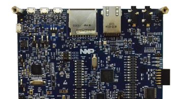
图.LPCXpresso54608/54618/54628评估板外形图(底视图)
详情请见:
责任编辑:HanFeng
【免责声明】
1、本文内容、数据、图表等来源于网络引用或其他公开资料,版权归属原作者、原发表出处。若版权所有方对本文的引用持有异议,请联系拍明芯城(marketing@iczoom.com),本方将及时处理。
2、本文的引用仅供读者交流学习使用,不涉及商业目的。
3、本文内容仅代表作者观点,拍明芯城不对内容的准确性、可靠性或完整性提供明示或暗示的保证。读者阅读本文后做出的决定或行为,是基于自主意愿和独立判断做出的,请读者明确相关结果。
4、如需转载本方拥有版权的文章,请联系拍明芯城(marketing@iczoom.com)注明“转载原因”。未经允许私自转载拍明芯城将保留追究其法律责任的权利。
拍明芯城拥有对此声明的最终解释权。


 产品分类
产品分类




 2012- 2022 拍明芯城ICZOOM.com 版权所有 客服热线:400-693-8369 (9:00-18:00)


