


 产品分类
产品分类
基于Microchip的PIC24FJ1024GB610 MCU开发方案
 254
254
 拍明
拍明
原标题:Microchip PIC24FJ1024GB610 MCU开发方案
microchip公司的PIC24FJ1024GB610是集成了闪存和USB OTG的16位微控制器(MCU).器件特性包括多达1024KB闪存,32KB RAM,USB和先进的外设,CPU采用修改的哈佛架构,32MHz时的性能高达16MIPS,主要用于工业计算,医疗/健身设备和需要长电池寿命的手持设备以及需要数据传输和存储如电表,HVAC控制,指纹扫描机和游戏机等.本文介绍了PIC24FJ1024GB610主要特性和框图,以及Explorer 16开发板主要特性,电路图和PCB元件布局图.
This powerful combination of features makes the PIC24F “GB6” family ideal for industrial, computer, medical/fitness and portable applications that require a long battery life, and data transfer and storage without the need of external memory, such as electricity metering, HVAC control, fingerprint scanners and gaming
PIC24F 16-bit Microcontroller featuring large dual partition flash with live update capability. This family includes up to 1024KB Flash, 32KB RAM, USB and advanced peripherals. The combination of features makes the part ideally suited for always on applications and applications requiring high memory.
The PIC24FJ1024GA610/GB610 family introducesmany new analog features to the extreme low-powerMicrochip devices. This is a 16-bit microcontroller familywith a broad peripheral feature set and enhancedcomputational performance. This family also offers a
new migration option for those high-performanceapplications which may be outgrowing their 8-bitplatforms, but do not require the numerical processingpower of a Digital Signal Processor (DSP).
PIC24FJ1024GB610主要特性:
High-Performance CPU
• Modified Harvard Architecture
• Largest Program Memory Available for PIC24(1024 Kbytes) for the Most Complex Applications
• 32 Kbytes SRAM for All Part Variants
• Up to 16 MIPS Operation @ 32 MHz
• 8 MHz Fast RC Internal Oscillator:
- 96 MHz PLL option
- Multiple clock divide options
- Run-time self-calibration capability for maintainingbetter than ±0.20% accuracy
- Fast start-up
• 17-Bit x 17-Bit Single-Cycle HardwareFractional/Integer Multiplier
• 32-Bit by 16-Bit Hardware Divider
• 16-Bit x 16-Bit Working Register Array
• C Compiler Optimized Instruction Set Architecture
• Two Address Generation Units for Separate Readand Write Addressing of Data Memory
Universal Serial Bus Features
• USB v2.0 On-The-Go (OTG) Compliant
• Dual Role Capable – Can Act as Either Host or Peripheral
• Low-Speed (1.5 Mb/s) and Full-Speed (12 Mb/s)
USB Operation in Host mode
• Full-Speed USB Operation in Device mode
• High-Precision PLL for USB
• USB Device mode Operation from FRC Oscillator –No Crystal Oscillator Required
• Supports up to 32 Endpoints (16 bidirectional):
- USB module can use any RAM location on thedevice as USB endpoint buffers
• On-Chip USB Transceiver with Interface for Off-ChipUSB Transceiver
• Supports Control, Interrupt, Isochronous andBulk Transfers
• On-Chip Pull-up and Pull-Down Resistors
Analog Features
• 10/12-Bit, up to 24-Channel Analog-to-Digital (A/D)Converter:
- 12-bit conversion rate of 200 ksps
- Auto-scan and threshold compare features
- Conversion available during Sleep
• Three Rail-to-Rail, Enhanced Analog Comparatorswith Programmable Input/Output Configuration
• Charge Time Measurement Unit (CTMU):
- Used for capacitive touch sensing, up to 24 channels
- Time measurement down to 100 ps resolution
High-Performance CPU
• Modified Harvard Architecture
• Largest Program Memory Available for PIC24(1024 Kbytes) for the Most Complex Applications
• 32 Kbytes SRAM for All Part Variants
• Up to 16 MIPS Operation @ 32 MHz
• 8 MHz Fast RC Internal Oscillator:
- 96 MHz PLL option
- Multiple clock divide options
- Run-time self-calibration capability for maintainingbetter than ±0.20% accuracy
- Fast start-up
• 17-Bit x 17-Bit Single-Cycle HardwareFractional/Integer Multiplier
• 32-Bit by 16-Bit Hardware Divider
• 16-Bit x 16-Bit Working Register Array
• C Compiler Optimized Instruction Set Architecture
• Two Address Generation Units for Separate Readand Write Addressing of Data Memory
Universal Serial Bus Features
• USB v2.0 On-The-Go (OTG) Compliant
• Dual Role Capable – Can Act as Either Host or Peripheral
• Low-Speed (1.5 Mb/s) and Full-Speed (12 Mb/s)USB Operation in Host mode
• Full-Speed USB Operation in Device mode
• High-Precision PLL for USB
• USB Device mode Operation from FRC Oscillator –No Crystal Oscillator Required
• Supports up to 32 Endpoints (16 bidirectional):
- USB module can use any RAM location on thedevice as USB endpoint buffers
• On-Chip USB Transceiver with Interface for Off-ChipUSB Transceiver
• Supports Control, Interrupt, Isochronous andBulk Transfers
• On-Chip Pull-up and Pull-Down Resistors
Analog Features
• 10/12-Bit, up to 24-Channel Analog-to-Digital (A/D)Converter:
- 12-bit conversion rate of 200 ksps
- Auto-scan and threshold compare features
- Conversion available during Sleep
• Three Rail-to-Rail, Enhanced Analog Comparatorswith Programmable Input/Output Configuration
• Charge Time Measurement Unit (CTMU):
- Used for capacitive touch sensing, up to 24 channels
- Time measurement down to 100 ps resolution
Peripheral Features
• Peripheral Pin Select (PPS) –Allows IndependentI/O Mapping of Many Peripherals
• Up to 5 External Interrupt Sources
• Configurable Interrupt-on-Change on All I/O Pins:
- Each pin is independently configurable for risingedge or falling edge change detection
• Eight-Channel DMA Supports All Peripheral modules:
- Minimizes CPU overhead and increases datathroughput
• Five 16-Bit Timers/Counters with Prescalers:
- Can be paired as 32-bit timers/counters
• Six Input Capture modules, Each with a Dedicated16-Bit Timer
• Six Output Compare/PWM modules, Each with aDedicated 16-Bit Timer
• Four Single Output CCPs (SCCPs) and ThreeMultiple Output CCPs (MCCPs):
- Independent 16/32-bit time base for each module
- Internal time base and period registers
- Legacy PIC24F Capture and Compare modes(16 and 32-bit)
- Special Variable Frequency Pulse and BrushlessDC Motor Output modes
• Enhanced Parallel Master/Slave Port (EPMP/EPSP)
• Hardware Real-Time Clock/Calendar (RTCC) withTimestamping
• Three 3-Wire/4-Wire SPI modules:
- Support 4 Frame modes
- 8-level FIFO buffer
- Support I2S operation
• Three I2C modules Support Multi-Master/Slavemode and 7-Bit/10-Bit Addressing
• Six UART modules:
- Support RS-485, RS-232 and LIN/J2602
- On-chip hardware encoder/decoder for IrDA®
- Auto-wake-up on Auto-Baud Detect (ABD)
- 4-level deep FIFO buffer
• Programmable 32-Bit Cyclic Redundancy Check(CRC) Generator
• Four Configurable Logic Cells (CLCs):
- Two inputs and one output, all mappable toperipherals or I/O pins
- AND/OR/XOR logic and D/JK flip-flop functions
• High-Current Sink/Source (18 mA/18 mA) on All I/O Pins
• Configurable Open-Drain Outputs on Digital I/O Pins
• 5.5V Tolerant Inputs on Multiple I/O Pins
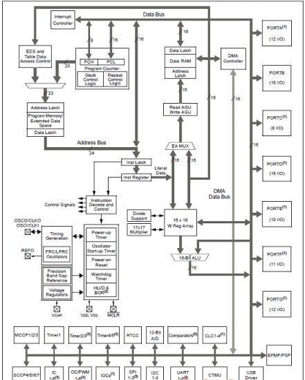
图1.PIC24FJ1024GB610/GA610系列框图
Explorer 16开发板
The Explorer 16 Development Board is a low-cost modular development system for Microchip’s 16-bit and 32-bit microcontrollers. It supports devices from the PIC24, dsPIC and PIC32 families. A variety of families are supported with processor Plug-In Modules (PIMs) for easy device swapping. The board includes a PICtail Plus daughter card connector for expansion boards including USB, CAN, Ethernet, wireless, graphics and many more. Coupled with the MPLAB ICD 3 In Circuit Debugger or MPLAB REAL ICE, real-time emulation and debug facilities speed evaluation and prototyping of application circuitry.
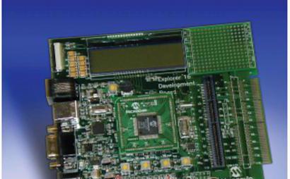
图2.Explorer 16开发板外形图
Explorer 16开发板主要特性:
Includes processor PIMs for both PIC24 and dsPIC families
Alpha-numeric 16 x 2 LCD display
Interfaces to MPLAB ICD 3, MPLAB REAL ICE and RS-232
Includes Microchip’s TC1047A high accuracy, analog output temperature sensor
Expansion connector to access full devices pin-out and bread board prototyping area
PICTailTM Plus connector for expansion boards
Full documentation in download section below: user’s guide, schematics
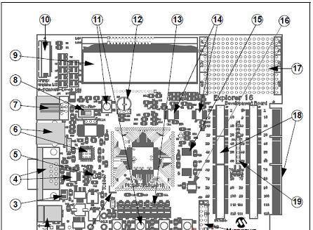
图3.Explorer 16开发板布局图
Explorer 16开发板中数字对应元件:
A layout of the Explorer 16 Development Board is shown in Figure 3. The boardincludes these key features, as indicated in the diagram:
1. 100-pin PIM riser, compatible with the PIM versions of selected MicrochipPIC MCU and dsPIC DSC devices
2. Direct 9 VDC power input that provides +3.3V and +5V (regulated) to the entireboard
3. Power indicator LED
4. RS-232 serial port and associated hardware
5. On-board analog thermal sensor
6. [No longer supported] USB connectivity for communications and devicEPROgramming/debugging
7. Standard, 6-wire In-Circuit Debugger (ICD) connector for connections to anMPLAB ICD programmer/debugger module
8. Hardware selection of PIM or soldered on-board microcontroller
9. 2-line by 16-character LCD
10. Provisioning on PCB for add on graphic LCD
11. Push button switches for device Reset and user-defined inputs
12. Potentiometer for analog input
13. Eight indicator LEDs
14. 74HCT4053 multiplexers for selectable crossover configuration on serial
communication lines
15. Independent crystals for precision microcontroller clocking (8 MHz) and RTCCoperation (32.768 kHz)
16. Serial EEPROM
17. Prototype area for developing custom applications
18. Socket and edge connector for PICtail™ Plus card compatibility
19. Six-pin interface for the PICkit™ Programmer
20. JTAG connector pad for optional boundary scan functionality
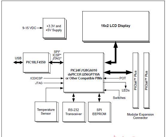
图4.Explorer 16开发板框图
责任编辑:HanFeng
【免责声明】
1、本文内容、数据、图表等来源于网络引用或其他公开资料,版权归属原作者、原发表出处。若版权所有方对本文的引用持有异议,请联系拍明芯城(marketing@iczoom.com),本方将及时处理。
2、本文的引用仅供读者交流学习使用,不涉及商业目的。
3、本文内容仅代表作者观点,拍明芯城不对内容的准确性、可靠性或完整性提供明示或暗示的保证。读者阅读本文后做出的决定或行为,是基于自主意愿和独立判断做出的,请读者明确相关结果。
4、如需转载本方拥有版权的文章,请联系拍明芯城(marketing@iczoom.com)注明“转载原因”。未经允许私自转载拍明芯城将保留追究其法律责任的权利。
拍明芯城拥有对此声明的最终解释权。
相关资讯
:
基于MC33771主控芯片的新能源锂电池管理系统解决方案

AMIC110 32位Sitara ARM MCU开发方案

基于AMIC110多协议可编程工业通信处理器的32位Sitara ARM MCU开发方案

基于展讯SC9820超低成本LTE芯片平台的儿童智能手表解决方案

基于TI公司的AM437x双照相机参考设计

基于MTK6580芯片的W2智能手表解决方案


 2012- 2022 拍明芯城ICZOOM.com 版权所有 客服热线:400-693-8369 (9:00-18:00)


