基于ADI公司的ADSP-CM41xF混合双核处理器开发方案
 543
543
 拍明
拍明
原标题:ADI ADSP-CM41xF混合双核处理器开发方案
ADI公司的ADSP-CM41xF系列混合信号控制处理器是基于ARM® Cortex-M4™处理器内核,带浮点单元,工作频率高达240 MHz,ARM® Cortex-M0™处理器内核工作频率高达100 MHz.处理器集成了许多业界领先的系统外设和丰富的存储器,在一个集成封装中提供RISC式编程能力和先进的信号处理能力,主要用在众多功率转换市场领域包括太阳能PV逆变器,电机/功率控制和电池充电/控制应用.本文介绍了ADSP-CM41xF主要特性包括系统特性和模拟前端特性,框图,双核ARM架构图和双核模拟前端框图,以及评估板ADSP-CM419F EZ-Kit特点,框图,电路图,材料清单和PCB设计图.
The ADSP-CM41xF family of mixed-signal control processorsis based on the ARM® Cortex-M4TM processor core with floatingpointunit operating at frequencies up to 240 MHz, and theARM® Cortex-M0TM processor core operating at frequencies upto 100 MHz. The processors integrate up to 160K Bytes ofSRAM memory with ECC, up to 1M Byte of flash memory withECC, accelerators and peripherals optimized for motor control and photo-voltaic (PV) inverter control, and an analog moduleconsisting of up to two 16-bit SAR-type ADCs, one 14-bit onM0 ADC and one 12-bit DAC. The ADSP-CM41xF familyoperates from a single voltage supply, generating its own internalvoltage supplies using internal voltage regulators and anexternal pass transistor.
By integrating a rich set of industry-leading system peripheralsand memory, the ADSP-CM41xF mixedsignalcontrol processors are the platform of choice fornext-generation applications that require RISC programmabilityand leading-edge signal processing in one integratedpackage. These applications span a wide array of markets in power conversion and include Solar PV inverters, motor/powercontrol, and battery charging/control.
ADSP-CM41xF主要特性:
系统特性:
Up to 240MHz ARM Cortex-M4 with floating-point unit withup to 160K Byte zero-wait-state ECC SRAM
Safety based dual-independent-core concept
Up to 1M Byte high performance ECC FLASH that can executeinstructions at near SRAM speed
Highest precision, low latency 31-channel analog front end
100 MHz ARM Cortex-M0 supervisor core with 32K Byte zerowait-state ECC SRAM
Single 3.3 V power supply
Static memory controller (SMC) with asynchronous memoryinterface that supports 8-bit and 16-bit memories
Enhanced,24-channel precision PWM unit
Four 3rd or 4th order SINC filters for glueless connection ofsigma-delta modulators
Hardware-based harmonic analysis engine
Logic block array (LBA)
FFT signal spectrum monitor
MATH function block
Two CAN 2.0B interfaces and up to five UARTs
Two serial peripheral interface (SPI-compatible) ports
Four encoder interfaces, two with frequency division
Package options:
176-lead (24 mm×24 mm) LQFP package
210-ball (15mm×15 mm) BGA package
模拟前端特性:
16-bit analog-to-digital converter with 24 multiplexed
inputs, supporting 6-way simultaneous sampling and
6-channel conversion in 1.4μ seconds
Independent 14-bit, 7-channel auxiliary analog-to-digital
converter with seven inputs
ADC controllers (ADCC0/ADCC1) and DAC controller (DACC0)
12-bit D/A converter
Up to three 2.5 V precision voltage reference outputs

图1.ADSP-CM41xF系列框图
ADSP-CM41xF products may contain one ARM Cortex-M4core, or may contain two ARM Cortex cores, an M4 and an M0.In dual core products, the system architecture is functionallypartitioned to allow each core reliable, independent operation. Using system protection resources (SPUs andSMPUs), the programmer can partition control of the systemresources arbitrarily among the two processors, down to thelevel of individual peripherals and to memory regions. Access toDMA slaves may be similarly regulated. Programmable bus timeoutprotection guarantees deterministic access completiontime between core domains even in the presence of hardwarefaults in one domain.
Each processor is equipped with its own essential infrastructure:
local SRAM, a set of communications peripherals (each has atleast one UART, CAN, and SPI,) a trigger routing unit (TRU), awatchdog timer (WDT), a system event controller (SEC), anADC controller (ADCC) and independent ADCs on the AFE,and a local APB and AXI bus fabric. The mailbox memory providesa shared memory bridge between the two subsystems forsemaphores and messages. A number of general-purpose interrupts and triggers cross between subsystems to allow selectedcommunication.
The main system AXI fabric provides universal memory interconnectbetween the two subsystems, displaying a unifiedmemory map to both processors containing all system resources(except those internal to or tightly coupled to the ARM cores).

图2.ADSP-CM41xF双核ARM架构图

图3.ADSP-CM418F/19F双核模拟前端框图

图4.ADSP-CM418F/19F典型电源配置图
评估板ADSP-CM419F EZ-Kit
The ADSP-CM419F EZ-Kit evaluation hardware is based on the ARM® Cortex®-M4 processor core with floating-point unit operating at frequencies up to 240 MHz, and the ARM® Cortex-M0TM processor core operating at frequencies up to 100 MHz. The EZ-Kit ships with all of the necessary hardware to get you up and running and start the evaluation immediately.
The EZ-KIT ships with all of the necessary hardware to get you up and running and start the evaluation immediately. The EZ-KIT contains an analog interface and PWM/digital interface. These interfaces are provided for connecting with daughter boards to expand on the functionality of the EZ-KIT. The evaluation board is designed to be used in conjunction with the IAR Embedded Workbench®andSegger® development environment for advanced application code development and debug such as:
Create, compile, assemble, and link application programs written in C++, C, and assembly
Load, run, step, halt, and set breakpoints in application programs
Read and write data and program memory
Read and write core and peripheral registers
评估板ADSP-CM419F EZ-Kit特点:
Analog Devices ADSP-CM419F processor
210 ball BGA
16 and 30 MHz oscillators
Analog Interface
Analog Devices Unity-Gain Stable, Ultralow Distortion, 1 nV/√Hz Voltage Noise, High Speed Op Amp (ADA4899)
Analog Devices Ultralow Noise, LDO XFET Voltage References with Current Sink and Source (ADR441B)
Analog Devices 1 ppm 20-Bit, ±1 LSB INL, Voltage Output DAC (AD5791)
LCD
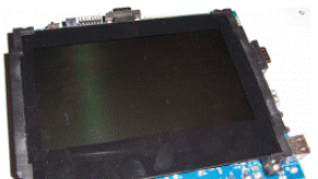
2.2 inch TFT LCD module
SPI Flash (SPI0) chip
Microchip 4K I2C Serial EEPROM (24AA04)
Universal Asynchronous Receiver/Transmitter (UART0)
Analog Devices Isolated Single Channel RS-232 Line Driver/Receiver (ADM3251E)
DB9
Universal Asynchronous Receiver/Transmitter (UART3)
FTDI USB to UART (FT232R)
USB mini-B
Universal Asynchronous Receiver/Transmitter (UART4)
Analog Devices Isolated, Dual Channel RS-232 Line Driver/Receiver (ADM3252E)
DB9
CAN
Analog Devices Signal and Power Isolated CAN Transceiver (ADM3053)
RJ11
SINC
Analog Devices Isolated, 5 kV, DC-to-DC Converter (ADUM6000)
Analog Devices Isolated Sigma-Delta Modulator (AD7401)
Debug (JTAG/SWD/SWO) interface
J-Link Lite emulator
JTAG/SWD/SWO 20-pin 0.1” header
JTAG/SWD/SWO 20-pin 0.05” header
LEDs - Five LEDs: one power (green),one board reset (red), two general-purpose (amber) and one fault (red)
Pushbuttons - Six pushbuttons: one reset and five IRQ/Flag
Analog connector
ADC
AGND/GND/VREF/5V
PWM connector
• PWM0-2
SINC0
SPI1
SPORT0
TWI0
TMR0
GPIOs
CNT0-3
RESET
GND/3.3V/5V output
External power supply
CE compliant
5V @3.6 Amps
Power measurement - 0.051-ohm resistors for measuring current draw

图5.评估板ADSP-CM419F EZ-Kit外形图

图6.评估板ADSP-CM419F EZ-Kit框图
评估板ADSP-CM419F EZ-Kit材料清单:


责任编辑:HanFeng
【免责声明】
1、本文内容、数据、图表等来源于网络引用或其他公开资料,版权归属原作者、原发表出处。若版权所有方对本文的引用持有异议,请联系拍明芯城(marketing@iczoom.com),本方将及时处理。
2、本文的引用仅供读者交流学习使用,不涉及商业目的。
3、本文内容仅代表作者观点,拍明芯城不对内容的准确性、可靠性或完整性提供明示或暗示的保证。读者阅读本文后做出的决定或行为,是基于自主意愿和独立判断做出的,请读者明确相关结果。
4、如需转载本方拥有版权的文章,请联系拍明芯城(marketing@iczoom.com)注明“转载原因”。未经允许私自转载拍明芯城将保留追究其法律责任的权利。
拍明芯城拥有对此声明的最终解释权。


 产品分类
产品分类




 2012- 2022 拍明芯城ICZOOM.com 版权所有 客服热线:400-693-8369 (9:00-18:00)


