基于NXP公司的QN9020超低功耗蓝牙(BLE)系统级芯片解决方案
 812
812
 拍明
拍明
原标题:NXP QN9020超低功耗蓝牙(BLE)系统级芯片解决方案
NXP公司的QN902x系列产品是超低功耗高性能和高度集成的蓝牙(BLE)系统级芯片(SoC),集成了BLE无线电(2400MHz-2483.5MHz),控制器,协议堆栈和基本应用软件,空中数据速率1Mbps,间隔250kHz.此外还集成了高性能MCU和存储器,支持用于开发单片无线MCU解决方案.主要用于运动和健身设备,医疗保健,遥控,智能手机配件,PC外设和无线传感器网络(WSN).本文介绍了QN902x系列主要特性和优势,框图和多种应用电路及所用外接元件, 开发板QN9020DK主要特性,电路图和PCB元件布局图.
QN902x is an ultra low power, high performance and highly integrated Bluetooth LE solution. It is used in Bluetooth Smart applications such as sports and fitness, human interface devices, and app-enabled smart accessories. It is specially designed for
wearable electronics and can run on a small capacity battery such as a coin cell battery.
QN902x integrates a Bluetooth LE radio, controller, protocol stack and profile software on
a single chip, providing a flexible and easy to use Bluetooth LE SoC solution. It also has a
high performance MCU and an on-chip memory that can support users to develop a
single-chip wireless MCU solution. Users can also utilize QN902x as a network processor
by connecting to an application processor for more advanced applications.
Additional system features include fully integrated DC-to-DC converter and LDO,
low-power sleep timer, battery monitor, general-purpose ADC, and GPIOs. These features
reduce overall system cost and size. QN902x has very low power consumption in all
modes. It enables long life in battery-operated systems while maintaining excellent RF
performance. QN9020/1 operates with a power supply range of 2.4 V to 3.6 V. The
QN9022 operates with a power supply range of 1.8 V to 3.6 V.
QN902x系列主要特性和优势:
True single-chip Bluetooth LE SoC solution
Integrated Bluetooth LE radio
Complete Bluetooth LE protocol stack and application profiles
Supports both master and slave modes
Up to eight simultaneous links in master mode
frequency bands: 2400 MHz to 2483.5 MHz
1 Mbit/s on air data rate and 250 kHz deviation
GFSK modulation format
RF
95 dBm RX sensitivity (non-DC-to-DC mode)
93 dBm RX sensitivity (DC-to-DC mode)
TX output power from 20 dBm to +4 dBm
Fast and reliable RSSI and channel quality indication
Compatible with worldwide radio frequency regulations
Excellent link budget up to 99 dB
Very low power consumption
Single power supply of 2.4 V to 3.6 V for QN9020/1
Single power supply of 1.8 V to 3.6 V for QN9022
Integrated DC-to-DC converter and LDO
2 uA deep sleep mode
3 uA sleep mode (32 kHz RC oscillator on)
9.25 mA RX current with DC-to-DC converter
8.8 mA TX current @0 dBm TX power with DC-to-DC converter
Compact 6 mm x 6 mm HVQFN48 package for QN9020, 5 mm x 5 mm HVQFN32
package for QN9021, and 5 mm x 5 mm HVQFN40 package for QN9022
Microcontroller
Integrated 32-bit ARM Cortex-M0 MCU
64 kB system memory
User-controllable code protection
High-level integration
4-channel, 10-bit general-purpose ADC
Two general-purpose analog comparators
31 GPIO pins for QN9020, 15 GPIO pins for QN9021, and 22 GPIO pins for
QN9022
GPIO pins can be used as interrupt sources
Four general-purpose timers
32 kHz sleep timer
Watchdog timer
Real-time clock with calibration
2-channel programmable PWM
Two SPI/UART interfaces
I2C-bus master/slave interface
Brownout detector
Battery monitor
AES-128 security coprocessor
16 MHz or 32 MHz crystal oscillator
Low power 32 kHz RC oscillator
32.768 kHz crystal oscillator
QN902x系列应用:
Sports and fitness
Healthcare and medical
Remote control
Smartphone accessories
PC peripherals (mouse and keyboard)
Wireless sensor networks

图1. QN902x系列框图

图2. QN9020带DC/DC转换器典型应用电路

图3. QN9020不带DC/DC转换器典型应用电路

图4. QN9021带DC/DC转换器典型应用电路

图5. QN9021不带DC/DC转换器典型应用电路

图6. QN9022带DC/DC转换器典型应用电路

图7. QN9022不带DC/DC转换器典型应用电路
QN902x系列产品应用电路外接元件列表:

开发板QN9020DK
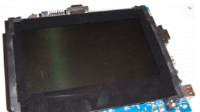
The QN9020DK board is designed to make it as easy as possible to get started with your project based on NXP QN9020 BLE SOC.
The QN9020DK board integrates buttons, Piezo buzzer, LED for easy way to reset chip and indicate chip status. The DK board also provides useful interfaces such as USB port for UART communication and JLink debug, GPIO sensor.

图8. 开发板QN9020DK外形图
开发板QN9020DK主要特性:
Contains Jlink-OB offering SWD and UART interfaces for QN9020 debug and communication
Mini USB port for power and communication port
Power source select jumper used for power source selection
Current measurement jumpers used for measuring the QN9020 device power consumption
Button1/2 used as input
LED1/2 used as output to indicate QN9020 status
Extended QN9020 GPIO Port used for interface extension
UART interface used as communication port for QN9020 device
Kit Contains
QN9020 DK Board
QN9020 USB dongle
USB cable
责任编辑:HanFeng
【免责声明】
1、本文内容、数据、图表等来源于网络引用或其他公开资料,版权归属原作者、原发表出处。若版权所有方对本文的引用持有异议,请联系拍明芯城(marketing@iczoom.com),本方将及时处理。
2、本文的引用仅供读者交流学习使用,不涉及商业目的。
3、本文内容仅代表作者观点,拍明芯城不对内容的准确性、可靠性或完整性提供明示或暗示的保证。读者阅读本文后做出的决定或行为,是基于自主意愿和独立判断做出的,请读者明确相关结果。
4、如需转载本方拥有版权的文章,请联系拍明芯城(marketing@iczoom.com)注明“转载原因”。未经允许私自转载拍明芯城将保留追究其法律责任的权利。
拍明芯城拥有对此声明的最终解释权。


 产品分类
产品分类




 2012- 2022 拍明芯城ICZOOM.com 版权所有 客服热线:400-693-8369 (9:00-18:00)


