


 产品分类
产品分类
基于Microsemi的SmartFusion2 SoC FPGA系列安全评估方案
 391
391
 拍明
拍明
原标题:Microsemi SmartFusion2 SoC FPGA系列安全评估方案
Microsemi公司的SmartFusion2 SoC FPGA系列是提供多达90K逻辑单元,多达5MB嵌入RAM,多达4个SERDES通路,多达2个PCIe端点,集成了具有单误差修正和双误差检测的硬DDR3存储器控制器,并提供了带嵌入ARM® Cortex™-M3的低功耗实时MCU子系统(MSS),主要用通信,工业,医疗,国防和航空等市场.本文介绍了SmartFusion2 SoC FPGA系列主要特性和架构图,SmartFusion2安全评估板M2S090TS-EVAL-KIT主要特性,框图,电路图和材料清单,PCB元件布局图.
Microsemi®’s automotive grade SmartFusion®2 system-on-chip (SoC) field programmable gate array (FPGA) andiglOO®2 FPGA families offer the best-in-class security, industry leading high reliability and lowest static power in aflash-based fabric. With a strong heritage of supplying to Military and Aviation customers, Microsemi automotive gradedevices are ideally suited to meet the demands of the automotive industry providing the lowest total-cost-of-ownership.
These next-generation devices integrate an industry standard 4-input lookup table-based (LUT) FPGA fabric withintegrated mathblocks, multiple embedded memory blocks, high-performance SERDES communications interfaces ona single chip with extended temperature support.
Automotive grade SmartFusion2 and IGLOO2 devices offer up to 90 K Logic Elements, up to 5 MB of embedded RAM,up to 4 SERDES lanes, up to 2 PCIe endpoints and integrated hard DDR3 memory controllers with single error correctand double error detect. IGLOO2 automotive grade devices integrate a high-performance memory subsystem (HPMS)with on-chip flash, 32 kbyte embedded SRAM, and multiple DMA controllers. SmartFusion2 automotive grade SoCFPGAs provide a low-power real time microcontroller subsystem (MSS) with an embedded ARM® Cortex™-M3encapsulating the benefits of HPMS along with a rich set of industry standard peripherals including Ethernet, USB, andCAN.
SmartFusion2 and IGLOO2 FPGAs are the best alternative to ASICs and SRAM based FPGAs with their advantagesof Zero FIT reliability, tamper-free advanced security, industry’s lowest static power and supply assurance for longproduct lifetime support.
Microsemi SmartFusion2 SoC FPGAs Offer More Resources in Low Density Devices With The Lowest Power, Proven Security and Exceptional Reliability .
These flash FPGA devices are ideal for general purpose functions such as Gigabit Ethernet or dual PCI Express control planes, bridging functions, input/output (I/O) expansion and conversion, video/image processing, system management and secure connectivity. Microsemi FPGAs are used by customers in munications, Industrial, Communications, Industrial, Medical, Defense, and Aviation markets.
SmartFusion2 SoC FPGA系列主要特性:
More Resources in Low Density Devices
ARM Cortex-M3 Processor with embedded flash
Comprehensive microcontroller subsystem
PCIe Gen2 support in 10K LE
With Clear Advantages
Lowest Power
Reduce total power by ~20-40%
70mW per 5G SERDES
Proven Security
Protection from Overbuilding and Cloning
Secure Boot for FPGA & Processors
Exceptional Reliability
SEU immune Zero FIT Flash FPGA Configuration
Reliability safety critical and mission critical systems
SmartFusion2 SoC FPGA架构
SmartFusion2 SoC FPGAs offer 5K-150K LEs with a 166MHz ARM® Cortex™-M3 processor, including ETM and Instruction Cachewith on-chip eSRAM&eNVM and a complete Microcontroller Subsystem with extensive peripherals including CAN, TSE, USB. Architecture highlights include:
• 16x 5Gbps SERDES, PCIe, XAUI / XGXS+ Native SERDES
• Up to 150K LEs, 5Mbit SRAM, 4Mbit eNVM
• Hard 667 mbps DDR2/3 controllers
• Integrated DSP processing blocks
• Power as low as 7mW Standby, Typical
• DPA Hardened, AES256, SHA256, On-Demand NVM Data Integrity Check
• SEU Protected/Tolerant Memories: eSRAMs, DDR Bridges
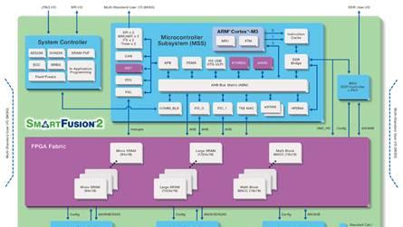
图1.SmartFusion2 SoC FPGA系列框图
SmartFusion2安全评估板M2S090TS-EVAL-KIT
The SmartFusion®2 system-on-chip (SoC) field programmable gate array (FPGA) Security Evaluation Kit (M2S090TS-EVAL-KIT) is restriction of hazardous substances (RoHS) compliant and enables you to develop applications that involve the following:
• Data security
• Motor control
• System management
• Industrial automation
• High-speed serial I/O applications:
− Peripheral component interconnect express (PCIe)
− Serial gigabit media independent interface (SGMII)
− User customizable serial interfaces
The M2S090TS-EVAL-KIT offers a full-featured Evaluation Board for SmartFusion2 SoC FPGAs. This board has the following features integrated on a single chip:
• Reliable flash-based FPGA fabric
• 166 MHz ARM® Cortex®-M3 processor
• Advanced security processing accelerators
• Digital signal processing (DSP) blocks
• Static random-access memory (SRAM)
• Embedded non-volatile memory (eNVM)
• High-performance communication interfaces
The SmartFusion2 Security Evaluation board has numerous standard interfaces such as:
• An RJ45 for 10/100/1000 Ethernet
• One full-duplex serializer/deserializer (SERDES) lane through sub-miniature version A (SMA) connectors
• A 64-bit GPIO Header
• Various connectors for serial peripheral interface (SPI) support
The SmartFusion2 memory management system supports 512 Mb on-board low-power double data rate (LPDDR) SDRAM memory and 64 Mb SPI flash memory. The SERDES block can be accessed using the PCIe edge connector or high-speed SMA connectors.
The board supports the M2S090TS device in an FGG484 package. The PCB has eight layers and manufactured with FR4 dielectric material.
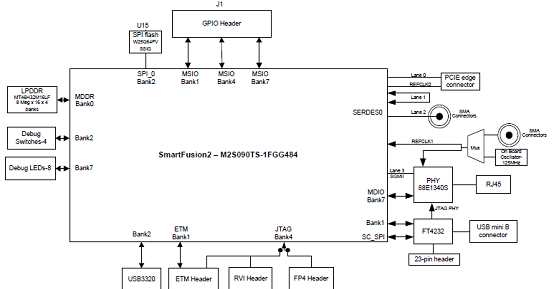
图2.安全评估板M2S090TS-EVAL-KIT框图
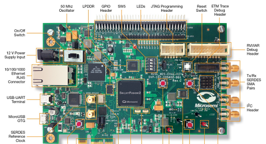
图3.安全评估板M2S090TS-EVAL-KIT外形
责任编辑:HanFeng
【免责声明】
1、本文内容、数据、图表等来源于网络引用或其他公开资料,版权归属原作者、原发表出处。若版权所有方对本文的引用持有异议,请联系拍明芯城(marketing@iczoom.com),本方将及时处理。
2、本文的引用仅供读者交流学习使用,不涉及商业目的。
3、本文内容仅代表作者观点,拍明芯城不对内容的准确性、可靠性或完整性提供明示或暗示的保证。读者阅读本文后做出的决定或行为,是基于自主意愿和独立判断做出的,请读者明确相关结果。
4、如需转载本方拥有版权的文章,请联系拍明芯城(marketing@iczoom.com)注明“转载原因”。未经允许私自转载拍明芯城将保留追究其法律责任的权利。
拍明芯城拥有对此声明的最终解释权。
相关资讯
:
基于MC33771主控芯片的新能源锂电池管理系统解决方案

AMIC110 32位Sitara ARM MCU开发方案

基于AMIC110多协议可编程工业通信处理器的32位Sitara ARM MCU开发方案

基于展讯SC9820超低成本LTE芯片平台的儿童智能手表解决方案

基于TI公司的AM437x双照相机参考设计

基于MTK6580芯片的W2智能手表解决方案


 2012- 2022 拍明芯城ICZOOM.com 版权所有 客服热线:400-693-8369 (9:00-18:00)


