基于Cypress公司的S6E2DF 32位图像MCU入门开发方案
 212
212
 拍明
拍明
原标题:Cypress S6E2DF 32位图像MCU入门开发方案
cypress公司的S6E2DF系列是高度集成的基于ARM Cortex-M4F处理器的32位MCU,工作频率高达160MHz,内置了FPU,支持DSP指令,通时集成了384KB闪存和SRAM,非常适合带TFT显示器的嵌入应用如家用电器,多功能打印机,工业设备,电子音乐设备和安全系统.本文介绍了S6E2DF主要特性,框图,以及带WQVGA TFT显示器的FM4-176L-S6E2DH图像MCU入门板主要特性和电路图.
Devices in the S6E2DFSeries are highly integrated 32-bit microcontrollers with high performance and competitive cost.This series isbased on the ARM Cortex-M4F Processor with on-chip Flash memory and SRAM.The series hasperipheral functions such as graphics engine, display controller, motor control timers, ADCs,and Communication Interfaces (USB, UART, CSIO, I2C, LIN).The productsthatare described in this data sheet are TYPE4-M4 category products. See the FM4 Family Peripheral Manual Main Part (002-04856).
S6E2DF主要特性:
32-bit ARM Cortex-M4F Core
Processor version: r0p1
Up to 160 MHz frequency operation
Built-in FPU
Supports DSP instructions
Memory Protection Unit (MPU): improves the reliability of an embedded system
Integrated Nested Vectored Interrupt Controller (NVIC): 1 NMI (non-maskable interrupt) and 128 peripheral interrupts and 16 priority levels
24-bit system timer (Sys Tick): System timer for OS task management
On-Chip Memories
Flash memory
This series has on-chip flash memory with these features:
384 Kbytes
Built-in Flash Accelerator System with 16 Kbytes trace buffer memory
Security function for code protection
Notes:
• The read access to flash memory can be achieved without wait-cycle up to operation frequency of 72 MHz.
• Even at the operation frequency more than 72 MHz, an equivalent access to flash memory can be obtained by Flash Accelerator System.
SRAM
This is composed of twoindependent SRAMs (SRAM0 and SRAM2). SRAM0 is connected toI-code bus and D-code bus of Cortex-M4F core. SRAM2 isconnected to the system bus ofCortex-M4F core.
SRAM0:32 Kbytes
SRAM2: 4 Kbytes
VRAM
This series is equipped with a SRAM for GDC.
Max 512 Kbytes
VFLASH
S6E2DF5GJA is equipped with a Flashfor GDC.
2 Mbytes
External Bus Interface
Supports SRAM, NOR, NAND Flash and SDRAM devices
Up to twochip selects CS0 andCS8 (CS8 is only for SDRAM)
8-/16-bit data width
Up to 25-bit address bit
Maximum area size : Up to 256 Mbytes
Supports address/data multiplexing
Supports external RDY function
Supports the scramble function
Possible to set the validity/invalidity of the scramble function for the external areas 0x6000_0000 to 0x7FFF_FFFF in 4 Mbytes units.
Possible to set two kinds of the scramble key.
Note:It is necessary to prepare the dedicated software library to use the scramble function.
USB Interface (One channel)
A USB interface is composed of deviceandhost.
USB device
USB2.0 Full-Speed supported
Max 6 EndPoint supported
• EndPoint 0 is for control transfer
• EndPoint 1, 2 can be selected for bulk-transfer, interrupt-transfer or isochronous-transfer
• EndPoint 3 to 5 can select bulk-transfer or interrupt-transfer
EndPoint 1 to 5 comprise the double buffer
The size of each endpoint is as follows.
• Endpoint0, 2to 5: 64bytes
• EndPoint 1: 256bytes
USB host
USB2.0 Full-Speed / Low-Speedsupported
Bulk-transfer, interrupt-transfer and isochronous-transfer support
USB device connected/disconnected automatically detect
In/outtoken handshake packet automaticallyaccepted
Max 256-byte packet-length supported
Wake-up function supported
Multi-function Serial Interface (Maxeightchannels)
64 bytes with FIFO(the FIFO step numbers varydepending on the settings of the communicationmode or bit length.)
Operation mode is selectable from the following for each channel.
UART
CSIO
LIN
I2C
UART
Full-duplex double buffer
Selection with or without parity supported
Built-in dedicated baud rate generator
External clock available as a serial clock
Various error detect functions available (parity errors, framing errors, and overrun errors)
CSIO
Full-duplex double buffer
Built-in dedicated baud rate generator
Overrun error detect function available
Serial chip select function (ch.6 and ch.7 only)
Supports High-speed SPI (ch.6 only)
Data length 5 to 16-bit
LIN
LIN protocol Rev.2.1 supported
Full-duplex double buffer
Master/Slave mode supported
LINbreak field generation (can change to 13 to 16-bit length)
LIN break delimiter generation (can change to 1 to 4-bit length)
Various error detect functions available (parity errors, framing errors, and overrun errors)
I2C
Standard mode (Max 100 kbps) / Fast mode (Max 400 kbps) supported
Fast mode Plus (Fm+) (Max 1000 kbps, only for ch.4=ch.A) supported
DMA Controller (Eightchannels)
The DMA controller has an independent bus for the CPU, so the CPU and the DMA controller can process simultaneously.
8 independently configured and operated channels
Transfer can be started by software or requestedfrom the built-in peripherals
Transfer address area: 32-bit (4 Gbytes)
Transfer mode: Block transfer/Burst transfer/Demand transfer
Transfer data type: bytes/half-word/word
Transfer block count: 1 to 16
Number of transfers: 1 to 65536
DSTC (Descriptor System Data Transfer Controller) (128 channels)
The DSTC can transfer data at high-speed without going via the CPU. The DSTC adopts the descriptorsystem and, following the specified contents of the descriptor thathas already been constructed onthememory, can directly access the memory/peripheral device and performs the data transfer operation.
It supports the software activation, the hardware activationand the chain activation functions.
A/DConverter (Max 24 channels)
12-bit A/D Converter
Successive Approximation type
Built-in 2units
Conversion time: 1.0 μs @ 3.3 V
Priority conversion available (priority at two levels)
scanning conversion mode
Built-in FIFO for conversion data storage (for SCAN conversion: 16steps, for priority conversion: four steps)
Base Timer (Max eightchannels)
Operation mode is selectable from the followings for each channel.
16-bit PWM timer
16-bit PPG timer
16-/32-bit reload timer
16-/32-bit PWC timer
General-Purpose I/O Port
This series can use its pins as general-purpose I/O ports when they are not used for external bus orperipherals. Moreover, the port relocate function is built in. It can set to which I/O port the peripheral functioncan be allocated.
Capable of pull-up control per pin
Capable of reading pin level directly
Built-in port relocate function
Up to 98general-purpose I/O ports @ 120-pin package
Some I/O pins are5V tolerant.See "4. PinDescriptions" and "5.I/O CircuitType"for the corresponding pins.
Multi-Function Timer (One unit)
The multi-function timer is composed of the following blocks.
Minimum resolution : 6.25 ns
16-bit free-run timer × 3ch.
Input capture × 4ch.
Output compare × 6ch.
A/D activation compare × 6ch.
Waveform generator × 3ch.
16-bit PPG timer × 3ch.
The following functionscan be used to achieve motor control.
PWM signal output function
DC chopper waveform output function
Dead time function
Input capture function
A/D converter activate function
DTIF (motor emergency stop) interrupt function
Real-Time Clock (RTC)
The real-time clock can count Year/Month/Day/Hour/Minute/Second/A day of the week from 01 to 99.
Interrupt function with specifying date and time (Year/Month/Day/Hour/Minute/Second/A day of theweek.) is available. This function is also available by specifying only Year, Month, Day, Hour or Minute.
Timer interrupt function after set time or each set time.
Capable of rewriting the time with continuing the time count.
Leap year automatic count is available.
Quadrature Position/Revolution Counter (QPRC) (Onechannel)
The Quadrature Position/Revolution Counter (QPRC) is used to measure the position of the positionencoder. Moreover, it is possible to useup/down counter.
The detection edge of the three external event input pins AIN, BIN and ZIN is configurable.
16-bit position counter
16-bit revolution counter
Two 16-bit compare registers
Dual Timer (32-/16-bit Down Counter)
The dual timer consists of twoprogrammable 32-/16-bit down counters.Operation mode is selectable from the followings for each channel.
Free-running
Periodic (=Reload)
One-shot
Watch Counter
The watch counter is used for wake up from the low-power consumption mode. It is possible to select themain clock, sub clock, built-in High-speed CR clock or built-in Low-speed CR clock as the clock source.
Interval timer: up to 64s (Max) @ Sub Clock: 32.768 kHz
Watchdog Timer (Twochannels)
A watchdog timer can generate interrupts or a reset when a time-out value is reached.
This series consists of two different watchdogs, a hardwarewatchdog and a software watchdog.
The hardware watchdog timer is clocked by low-speed internal CR oscillator. Therefore, the hardware watchdog is active in any power saving mode except RTC mode and stop mode.
CRC (Cyclic Redundancy Check) Accelerator
The CRC accelerator helps verify data transmission or storage integrity.
CCITT CRC16 and IEEE-802.3 CRC32 are supported.
CCITT CRC16 Generator Polynomial: 0x1021
IEEE-802.3 CRC32 Generator Polynomial: 0x04C11DB7
PRGCRC(Programmable Cyclic Redundancy Check)Accelerator
The CRC accelerator helpsverify data transmission or storage integrity.
CCITT CRC16, IEEE-802.3 CRC32and a generating polynominal are supported.
CCITT CRC16 Generator Polynomial: 0x1021
IEEE-802.3 CRC32 Generator Polynomial: 0x04C11DB7
Generating polynominal
SD Card Interface
It is possible to use the SD card that conforms to the following standards.
Part 1 Physical Layer Specification version 3.01
Part E1 SDIO Specification version 3.00
Part A2 SD Host Controller Standard Specification version 3.00
1-bit or 4-bit data bus
I2S Interface (TX x twochannels, RX x twochannels)
Support three transfer protocols
I2S
Left Justified
DSP mode
Master/Slave Mode selectable
RX only, TX only or TX and RX simultaneous operation selectable
Word length is programmable from 7bits to 32bits
RX/TXFIFO integrated (RX: 66 words x 32bits, TX: 66 words x 32bits)
DMA, interrupts,or polling based data transfer supported
GDC Unit
Controller for external graphics display
Accelerator for 2D block image transfer (blit) operations
Embedded SRAM video memory
High-Speed Quad SPI (Serial Peripheral Interface for external memory extensions)
SDRAM interface for external memory extensions
HBI (Hyper Bus Interface) interface for external memory extensions
Maximum core system clock frequency : 160 MHz
Clock and Reset
Clocks
Five clock sources (twoexternal oscillators, twointernal CR oscillator, and Main PLL) that are dynamicallyselectable.
Main clock: 4MHzto 20 MHz
Sub Clock: 32.768kHz
High-speed internal CR Clock: 4MHz
Low-speed internal CR Clock: 100kHz
Main PLL Clock
Resets
Reset requests from INITX pin
Power on reset
Software reset
Watchdog timers reset
Low voltage detector reset
Clock supervisor reset
Clock Super Visor (CSV)
Clocks generated by internal CR oscillators are used to supervise abnormality of the external clocks.
External OSC clock failure (clock stop) is detected, reset is asserted.
External OSC frequency anomaly is detected, interrupt or reset is asserted.
Low-Voltage Detector (LVD)
This Series include 2-stage monitoring of voltage on the VCC pins. When the voltage falls below thevoltage has been set, Low-Voltage Detector generates an interrupt or reset.
LVD1: error reporting via interrupt
LVD2: auto-reset operation
Low-Power Consumption Mode
Six low-power consumption modes are supported.
Sleep
Timer
RTC
Stop
Deep standby RTC (selectable from with/without RAM retention)
Deep standby Stop(selectable from with/without RAM retention)
Peripheral Clock Gating
The system canreducethe current consumption of the total systemwith gating the operation clocks of peripheralfunctions not used.
VBAT
The consumption power during the RTC operation can be reduced by supplying the power supplyindependent from the RTC (calendar circuit)/32 kHz oscillation circuit. The following circuits can also beused.
RTC
32 kHz oscillation circuit
Power-on circuit
Back up register : 32 bytes
Port circuit
Debug
Serial Wire Debug Port (SWJ-DP)
Embedded Trace Macrocells (ETM) provide comprehensive debug and trace facilities.
Unique ID
Unique value ofthe device (41-bit) is set.
Power Supply
Two Power Supplies
Power supply:
VCC= 2.7Vto 3.6 V(when USBor GDC unitis not used)
= 3.0V to 3.6V (when USBor GDC unit is used)
Power supply for VBAT:
VBAT= 1.65Vto 3.6 V

图1.S6E2DF框图
带WQVGA TFT显示器的FM4-176L-S6E2DH图像MCU入门板
FM4-176L-S6E2DH - ARM® Cortex®-M4 FM4 Graphics MCU Starter Kit with WQVGA TFT Display
The Spansion® S6E2DH series graphics controller MCU starter kit provides an easy to use, cost-effective solution to evaluate an ARM® Cortex®-M4 based microcontroller that incorporates a dedicated hardware graphics engine allowing rich display images. The board comes complete with WQVGA TFT display with a touch sensor and on-board CMSIS-DAP enabling the user to connect directly to a PC and begin development. In addition to the evaluation board, the Spansion solution includes a free-of-charge graphics authoring tool and low-level libraries for the graphics engine.
Spansion’s S6E2DH MCU is ideal for embedded applications with TFT displays such as home appliances, multi-function printers, industrial equipment, electronic musical instruments and security systems.
FM4-176L-S6E2DH图像MCU入门板主要特性:
• Spansion FM4 S6E2DH MCU
• CMSIS-DAP JTAG adapter
• USB-Device (Type-B connector)
• WQVGA TFT Panel with touch
• 512MB SpansionHyperFlash™ memory for image storage
• 128MB SDRAM for external VRAM
• I2S connection to codec
• SD card interface
Order number: SK-FM4-S6E2DH-TFT
The FM4-176L-S6E2DH board provides an easy-to-use low cost way to evaluate an ARM® Cortex®-M4 based microcontroller that incorporates a dedicated hardware graphics engine allowing rich display images. The board comes with a WQVGA TFT display equipped with touch sensor and external memory for image storage.
Featuring the FM4 ARM® Cortex®-M4 S6E2D-Series Graphics MCU
160MHz ARM® Cortex MCU with DMA
Graphics Display Controller (GDC) unit for external graphics display
Single precision IEEE 754 compliant floating point unit
2MB flash, 256KB SRAM and 154 GPIOs with additional 512KB SRAM and 2MB flash for GDC.
Communication interfaces: USB host, USB device, CAN, LIN, High-Speed Quad SPI, I2S, I2C and UART.
Featuring WQVGA TFT Display and HyperFlash for image storage
WQVGA TFT Panel with Touch
512 Mb HyperFlash™ and 128 Mb memory for image storage
I2S connection to codec
SD card interface

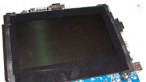
图2.FM4-176L-S6E2DH图像MCU入门板外形图

图3.FM4-176L-S6E2DH图像MCU入门板框图
详情请见:
![]() 002-05042_S6E2DF_Series_32-bit_ARM_R_Cortex_R_-M4F_FM4_Microcontroller.pdf
002-05042_S6E2DF_Series_32-bit_ARM_R_Cortex_R_-M4F_FM4_Microcontroller.pdf
责任编辑:HanFeng
【免责声明】
1、本文内容、数据、图表等来源于网络引用或其他公开资料,版权归属原作者、原发表出处。若版权所有方对本文的引用持有异议,请联系拍明芯城(marketing@iczoom.com),本方将及时处理。
2、本文的引用仅供读者交流学习使用,不涉及商业目的。
3、本文内容仅代表作者观点,拍明芯城不对内容的准确性、可靠性或完整性提供明示或暗示的保证。读者阅读本文后做出的决定或行为,是基于自主意愿和独立判断做出的,请读者明确相关结果。
4、如需转载本方拥有版权的文章,请联系拍明芯城(marketing@iczoom.com)注明“转载原因”。未经允许私自转载拍明芯城将保留追究其法律责任的权利。
拍明芯城拥有对此声明的最终解释权。


 产品分类
产品分类




 2012- 2022 拍明芯城ICZOOM.com 版权所有 客服热线:400-693-8369 (9:00-18:00)


