


 产品分类
产品分类
基于ST公司的STM32H743XI 32位400MHz ARM MCU开发方案
 275
275
 拍明
拍明
原标题:ST STM32H743XI 32位400MHz ARM MCU开发方案
ST公司的STM32H743XI是基于高性能的32位ARM Cortex-M7核的400MHz MCU,具有支持ARM双精度(IEEE 754兼容)和单精度数据处理指令和数据类型的浮点单元(FPU),支持所有DSP指令和存储器保护单元(MPU),闪存多达2MB和1MB RAM,所有的器件有三个ADC,两个DAC,两个超低功耗比较器,低功耗RTC,高分辨率计时器,12个通用16位计时器,用于马达控制的两个PWM计时器,五个低功耗计时器和随机码发生器(RNG),主要用在马达驱动和工业控制,医疗设备,工业应用如PLC,逆变器,电路中断器,打印机和扫描仪,告警系统,视频连接和HVAC,家庭音频设备,物联网和可穿戴如智能手表.本文介绍了STM32H743XI主要特性,框图以及评估板STM32H743I-EVAL主要特性,硬件框图和元件分布图以及电路图.
STM32H743xI devices are based on the high-performance ARM® Cortex®-M7 32-bit RISC core operating at up to 400 MHz.The Cortex® -M7 core features a floating point unit (FPU) which supports ARM® double-precision (IEEE 754 compliant) and single-precision data-processing instructions and data types. STM32H743xI devices support a full set of DSP instructions and a memory protection unit (MPU) to enhance application security.
STM32H743xI devices incorporate high-speed embedded memories with a dual-bank Flash memory up to 2 Mbytes, around 1 Mbyte of RAM (including 192 Kbytes of TCM RAM, 864 Kbytes of user SRAM and 4 Kbytes of backup SRAM), as well as an extensive range of enhanced I/Os and peripherals connected to APB buses, AHB buses, 2x32-bit multi-AHB bus matrix and a multi layer AXI interconnect supporting internal and external memory access.
All the devices offer three ADCs, two DACs, two ultra-low power comparators, a low-power RTC, a high-resolution timer, 12 general-purpose 16-bit timers, two PWM timers for motor control, five low-power timers, a true random number generator (RNG). The devices support four digital filters for external sigma-delta modulators (DFSDM). They also feature standard and advanced communication interfaces.
• Standard peripherals
– Four I2Cs – Four USARTs, four UARTs and one LPUART
– Six SPIs, three I2Ss in half-duplex mode. To achieve audio class accuracy, the I2S peripherals can be clocked by a dedicated internal audio PLL or by an external clock to allow synchronization.
– Four SAI serial audio interfaces
– One SPDIFRX interface
– One SWPMI (Single Wire Protocol Master Interface)
– Management Data Input/Output (MDIO) slaves
– Two SDMMC interfaces
– A USB OTG full-speed and a USB OTG high-speed interface with full-speed capability (with the ULPI) – One FDCAN plus one TT-CAN interface
– An Ethernet interface
– Chrom-ART Accelerator™
– HDMI-CEC
• Advanced peripherals including
– A flexible memory control (FMC) interface
– A Quad-SPI Flash memory interface
– A camera interface for CMOS sensors
– An LCD-TFT display controller
– A JPEG hardware compressor/decompressor
STM32H743xI devices operate in the –40 to +85 ℃ temperature range from a 1.62 to 3.6 V power supply. The supply voltage can drop down to 1.62 V by using an external power supervisor (see Section 3.5.2: Power supply supervisor) and connecting the PDR_ON pin to VSS. Otherwise the supply voltage must stay above 1.71 V with the embedded power voltage detector enabled.
Dedicated supply inputs for USB (OTG_FS and OTG_HS) are available on all packages except LQFP100 to allow a greater power supply choice.
A comprehensive set of power-saving modes allows the design of low-power applications.STM32H743xI devices are offered in 6 packages ranging from 100 pins to 240 pins/balls. The set of included peripherals changes with the device chosen.
These features make STM32H743xI microcontrollers suitable for a wide range of applications:
• Motor drive and application control
• Medical equipment
• Industrial applications: PLC, inverters, circuit breakers
• Printers, and scanners
• Alarm systems, video intercom, and HVAC
• Home audio appliances
• Mobile applications, Internet of Things
• Wearable devices: smart watches.
STM32H743XI主要特性:
Core
• 32-bit ARM® Cortex®-M7 core with double-precision FPU and L1 cache: 16 Kbytes of data and 16 Kbytes of instruction cache allowing one cache line to be filled in a single access from the 256-bit embedded Flash memory; frequency up to 400 MHz, MPU, 856 DMIPS/ 2.14 DMIPS/MHz (Dhrystone 2.1), and DSP instructions
Memories
• Up to 2 Mbytes of Flash memory with read-while-write support
• ~1 Mbyte of RAM: 192 Kbytes of TCM RAM (inc. 64 Kbytes of ITCM RAM + 128 Kbytes of DTCM RAM for time critical routines), 864 Kbytes of user SRAM, and 4 Kbytes of SRAM in Backup domain
• Dual mode Quad-SPI memory interface
• Flexible external memory controller with up to 32-bit data bus: SRAM, PSRAM, SDRAM/LPSDR SDRAM, NOR/NAND Flash
• CRC calculation unit
Security
• ROP, PC-ROP, active tamper, secure firmware upgrade support
General-purpose input/outputs
• Up to 168 I/O ports with interrupt capability
– Fast I/Os capable of up to 133 MHz
– Up to 164 5 V-tolerant I/Os
Reset and power management
• 3 separate power domains which can be independently clock gated or switched off to maximize power efficiency:
– D1: high-performance capabilities for high bandwidth peripherals
– D2: communication peripherals and timers
– D3: reset/clock control/power management
• 1.62 to 3.6 V application supply and I/Os
• POR, PDR, PVD and BOR
• Dedicated USB power embedding a 3.3 V internal regulator to supply the internal PHYs
• Embedded regulator (LDO) with configurable scalable output to supply the digital circuitry
• Voltage scaling in Run and Stop mode
• Backup regulator (~0.9 V)
• Voltage reference for analog peripheral and VREF+
• Low-power modes: Sleep, Stop and Standby
Low-power consumption
• Total current consumption down to 7 μA
Clock management
• Internal oscillators: 64 MHz HSI, 48 MHz HSI48, 4 MHz CSI, 40 kHz LSI
• External oscillators: 4-48 MHz HSE, 32.768 kHz LSE
• 3× PLLs (1 for the system clock, 2 for kernel clocks) with fractional mode
Interconnect matrix
• 3 bus matrices (1 AXI and 2 AHB)
• Bridges (5× AHB2-APB, 2× AXI2-AHB)
4 DMA controllers to unload the CPU
• 1× high-speed general-purpose master direct memory access controller (MDMA)
• 2× dual-port DMAs with FIFO and request router capabilities
• 1× basic DMA with request router capabilities
Up to 35 communication peripherals
• 4× I2C FM+ interfaces (SMBus/PMBus)
• 4× USART/4x UARTs (ISO7816 interface, LIN, IrDA, modem control) and 1x LPUART
• 6× SPIs, including 3 with muxed duplex I2S audio class accuracy via internal audio PLL or external clock and 1 x I2S in LP domain
• 4x SAIs (serial audio interface)
• SPDIFRX interface
• SWPMI single-wire protocol master I/F
• MDIO Slave interface
• 2× SD/SDIO/MMC interfaces
• 2× CAN controllers: 2 with CAN FD, 1 with time-triggered CAN (TT-CAN)
• 2× USB OTG interfaces (1FS, 1HS/FS)
• Ethernet MAC interface with DMA controller
• HDMI-CEC
• 8- to 14-bit camera interface up to 80 MHz
11 analog peripherals
• 3× ADCs with 16-bit max. resolution (14 bits 2.7 MSPS, 16 bits 168 kSPS)
• 1× temperature sensor
• 2× 12-bit D/A converters (1 MHz)
• 2× ultra-low-power comparators
• 2× operational amplifiers (8 MHz bandwidth)
• 1× digital filters for sigma delta modulator (DFSDM) with 8 channels/4 filters Graphics
• LCD-TFT controller up to XGA resolution
• Chrom-ART graphical hardware Accelerator™ (DMA2D) to reduce CPU load
• Hardware JPEG Codec
Up to 22 timers and watchdogs
• 1× high-resolution timer (2.5 ns max resolution)
• 2× 32-bit timers with up to 4 IC/OC/PWM or pulse counter and quadrature (incremental) encoder input
• 2× 16-bit advanced motor control timers
• 10× 16-bit general-purpose timers
• 5× 16-bit low-power timers
• 2× watchdogs (independent and window)
• 1× SysTick timer
• RTC with sub-second accuracy & HW calendar
Debug mode
• SWD & JTAG interfaces
• 4 Kbyte Embedded Trace Buffer
True random number generators (3 oscillators each) 96-bit unique ID
All packages are ECOPACK®2 compliant
STM32H743X评估板STM32H743I-EVAL
The STM32H743I-EVAL Evaluation board is a high-end development platform for the ARM® Cortex®-M7-based STM32H743XI microcontroller. The STM32H743I-EVAL Evaluation board provides access to all the STM32 peripherals for user applications and includes an embedded ST-LINK debugger/programmer. The full range of the hardware features on the STM32H743I-EVAL Evaluation board, helps to evaluate all the peripherals (USB OTG HS and FS, Ethernet, FD-CAN, USART, Audio DAC and ADC, digital microphone, SRAM, SDRAM, NOR Flash, Twin Quad-SPI Flash, microSD™ 3.0 card and 5.7” 640x480 TFT color LCD with touch screen) and to develop applications. The expansion connectors provide an easy way to add specialized features, while ETM trace is supported through external probes.
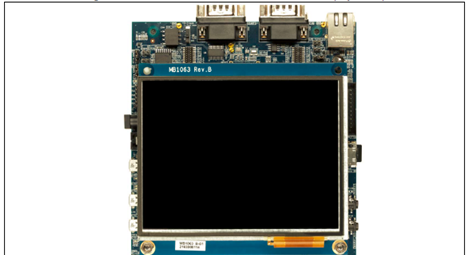
图.评估板STM32H743I-EVAL外形图
评估板STM32H743I-EVAL主要特性:
• STM32H743XIH6 microcontroller with 2 Mbytes of Flash memory and 1 Mbyte of RAM in TFBGA240+25 package
• 5.7” 640x480 TFT-color LCD with touch screen
• Ethernet compliant with IEEE-802.3-2002
• USB OTG HS and FS
• I2C compatible serial interface
• RTC with rechargeable backup battery
• SAI Audio DAC
• ST-MEMS digital microphones
• 8-Gbyte (or more) SDIO3.0 interface microSD™ card
• 8Mx32-bit SDRAM, 1Mx16bit SRAM and 8Mx16-bit NOR Flash
• 1 1-Gbit Twin Quad-SPI NOR Flash memory or two 512Mb Quad-SPI NOR Flash memories
• Potentiometer
• 4 colored LEDs
• Reset, wakeup, tamper or key buttons
• Joystick with 4-direction control and selector
• Board connectors
– Power jack
– 3 USB with Micro-AB
– RS-232 communications
– Ethernet RJ45
– FD-CAN compliant connection
– Stereo headset jack including analog microphone input
– 2 audio jacks for external speakers
– microSD™ card
– JTAG/SWD and ETM trace
• Board expansion connectors:
– Extension connectors and memory connectors for daughterboard or wire-wrap board
• Flexible power-supply options: ST-LINK USB VBUS or external sources
• On-board ST-LINK/V2-1 debugger/programmer with USB re-enumeration capability: mass storage, virtual COM port and debug port
• Comprehensive free software libraries and examples available with the STM32Cube package
详情请见:
责任编辑:HanFeng
【免责声明】
1、本文内容、数据、图表等来源于网络引用或其他公开资料,版权归属原作者、原发表出处。若版权所有方对本文的引用持有异议,请联系拍明芯城(marketing@iczoom.com),本方将及时处理。
2、本文的引用仅供读者交流学习使用,不涉及商业目的。
3、本文内容仅代表作者观点,拍明芯城不对内容的准确性、可靠性或完整性提供明示或暗示的保证。读者阅读本文后做出的决定或行为,是基于自主意愿和独立判断做出的,请读者明确相关结果。
4、如需转载本方拥有版权的文章,请联系拍明芯城(marketing@iczoom.com)注明“转载原因”。未经允许私自转载拍明芯城将保留追究其法律责任的权利。
拍明芯城拥有对此声明的最终解释权。
相关资讯
:
基于MC33771主控芯片的新能源锂电池管理系统解决方案

AMIC110 32位Sitara ARM MCU开发方案

基于AMIC110多协议可编程工业通信处理器的32位Sitara ARM MCU开发方案

基于展讯SC9820超低成本LTE芯片平台的儿童智能手表解决方案

基于TI公司的AM437x双照相机参考设计

基于MTK6580芯片的W2智能手表解决方案


 2012- 2022 拍明芯城ICZOOM.com 版权所有 客服热线:400-693-8369 (9:00-18:00)


