Microsemi ProASIC3L低功耗闪存FPGA解决方案
 156
156
 拍明
拍明
原标题:Microsemi ProASIC3L低功耗闪存FPGA解决方案
Microsemi公司的ProASIC3L是采用Flash*Freeze技术的低功耗闪存FPGA器件,和通常等价的ProASIC3相比,动态功耗降低40%,静态功耗降低50%,核工作电压1.2V-1.5V,I/O电压低至1.2V,提供1kb可重新编程非易失性FlashROM以及基于时钟调节电路的锁相环(PLL),支持250k到3百万系统门,多达504kb真双端SRAM和620个用户I/O,支持高性能32位Cortex-M1处理器.主要用在低功耗数据传输和控制,如手持媒体,安全通信,无线电应用以及高性能手持设备,工业,测试,科学和医疗设备.本文介绍了ProASIC3L主要特性和优势,架构图,以及Cortex-M1使能ProASIC3L开发板M1A3PL-DEV-KIT主要特性,框图和电路图与PCB元件分布图.
The ProASIC3L family of Microsemi flash FPGAs dramatically reduces dynamic power consumption by40% and static power by 50% compared to the equivalent ProASIC3 device. These power savings arecoupled with performance, density, true single-chip, 1.2 V to 1.5 V core and I/O operation as low as1.2 V, reprogrammability, and advanced features.
Using Microsemi’s proven Flash*Freeze technology enables users to shut off dynamic powerinstantaneously and switch the device to static mode without the need to switch off clocks or powersupplies while retaining internal states of the device. This greatly simplifies power management on aboard done through I/Os and clocks. In addition, optimized software tools using power-driven layoutprovide instant push-button power reduction.
Nonvolatile flash technology gives ProASIC3L devices the advantage of being a secure, low-power,single-chip solution that is Instant On. ProASIC3L offers dramatic dynamic power savings giving theFPGA users flexibility to combine low power with high performance.
These features enable designers to create high-density systems using existing ASIC or FPGA designflows and tools.ProASIC3L devices offer 1 kbit of on-chip, reprogrammable, nonvolatile FlashROM storage as well asclock conditioning circuitry (CCC) based on an integrated phase-locked loop (PLL). ProASIC3L devicessupport devices from 250 k system gates to 3 million system gates with up to 504 kbits of true dual-portSRAM and 620 user I/Os.
M1 ProASIC3L devices support the high-performance, 32-bit Cortex-M1 processor developed by ARMfor implementation in FPGAs. ARM Cortex-M1 is a soft processor that is fully implemented in the FPGAfabric. It has a three-stage pipeline that offers a good balance between low-power consumption andspeed when implemented in an M1 ProASIC3L device. The processor runs the ARMv6-M instruction set,has a configurable nested interrupt controller, and can be implemented with or without the debug block.
ARM Cortex-M1 is available for free from Microsemi for use in M1 ProASIC3L FPGAs.The ARM-enabled devices have MicrosemiSoC Products Group ordering numbers that begin with M1and do not support AES decryption.
The ProASIC3L devices offer Microsemi’s proven Flash*Freeze technology, which allows instantaneousswitching from an active state to a static state. ProASIC3L devices do not need additional components toturn off I/Os or clocks while retaining the design information, SRAM content, and registers. Flash*Freezetechnology is combined with in-system programmability, which enables users to quickly and easilyupgrade and update their designs in the final stages of manufacturing or in the field. The ability ofProASIC3L devices to support a wide range core voltage (1.2 V to 1.5 V) allows for an even greater reduction in power consumption, which enables low total system power.
When the ProASIC3L device enters Flash*Freeze mode, the device automatically shuts off the clocksand inputs to the FPGA core; when the device exits Flash*Freeze mode, all activity resumes and data isretained.
The availability of low-power modes, combined with a reprogrammable, single-chip, single-voltagesolution, make ProASIC3L devices suitable for low-power data transfer and manipulation in portablemedia, secure communications, radio applications as well as high performance portable, industrial,test,scientific, and medical applications.
ProASIC3L主要特性和优势:
Low Power
• Dramatic Reduction in Dynamic and Static Power Savings
• 1.2 V to 1.5 V Core and I/O Voltage Support for Low Power
• Low Power Consumption in Flash*Freeze Mode Allows forInstantaneous Entry to / Exit from Low-Power Flash*FreezeMode
• Supports Single-Voltage System Operation
• Low-Impedance Switches
High Capacity
• 250,000 to 3,000,000 System Gates
• Up to 504 kbits of True Dual-Port SRAM
• Up to 620 User I/Os
Reprogrammable Flash Technology
• 130-nm, 7-Layer Metal (6 Copper), Flash-Based CMOSProcess
• Instant On Level 0 Support
• Single-Chip Solution
• Retains Programmed Design when Powered Off
High Performance
• 350 MHz (1.5 V systems) and 250 MHz (1.2 V systems) SystemPerformance
• 3.3 V, 66 MHz, 66-Bit PCI (1.5 V systems) and 66 MHz, 32-BitPCI (1.2 V systems)
In-System Programming (ISP) and Security
• ISP Using On-Chip 128-Bit Advanced Encryption Standard(AES) Decryption via JTAG (IEEE 1532–compliant)
• FlashLock® to Secure FPGA Contents
High-Performance Routing Hierarchy
• Segmented, Hierarchical Routing and Clock Structure
• High-Performance, Low-Skew Global Network
• Architecture Supports Ultra-High Utilization
Advanced and Pro (Professional) I/Os
• 700 Mbps DDR, LVDS-Capable I/Os
• 1.2 V, 1.5 V, 1.8 V, 2.5 V, and 3.3 V Mixed-Voltage Operation
• Bank-Selectable I/O Voltages—up to 8 Banks per Chip
• Single-Ended I/O Standards: LVTTL, LVCMOS 3.3 V /2.5 V / 1.8 V / 1.5 V / 1.2 V, 3.3 V PCI / 3.3 V PCI-X, andLVCMOS 2.5 V / 5.0 V Input
• Differential I/O Standards: LVPECL, LVDS, B-LVDS, andM-LVDS
• Voltage-Referenced I/O Standards: GTL+ 2.5 V / 3.3 V, GTL2.5 V / 3.3 V, HSTL Class I and II, SSTL2 Class I and II, SSTL3Class I and II (A3PE3000L only)
• Wide Range Power Supply Voltage Support per JESD8-B,Allowing I/Os to Operate from 2.7 V to 3.6 V
• Wide Range Power Supply Voltage Support per JESD8-12,Allowing I/Os to Operate from 1.14 V to 1.575 V
• I/O Registers on Input, Output, and Enable Paths
• Hot-Swappable and Cold-Sparing I/Os Programmable OutputSlew Rate and Drive Strength
• Programmable Input Delay (A3PE3000L only)
• Schmitt Trigger Option on Single-Ended Inputs (A3PE3000L)
• Weak Pull-Up/-Down
• IEEE 1149.1 (JTAG) Boundary Scan Test
• Pin-Compatible Packages across the ProASIC®3L Family(except PQ208)
Clock Conditioning Circuit (CCC) and PLL
• Six CCC Blocks, One with Integrated PLL (ProASIC3L) and Allwith Integrated PLL (ProASIC3EL)
• Configurable Phase Shift, Multiply/Divide, Delay Capabilities,and External Feedback
• Wide Input Frequency Range 1.5 MHz to 250 MHz (1.2 Vsystems) and 350 MHz (1.5 V systems))
SRAMs and FIFOs
• Variable-Aspect-Ratio 4,608-Bit RAM Blocks (×1, ×2, ×4, ×9,and ×18 organizations available)
• True Dual-Port SRAM (except ×18)
• 24 SRAM and FIFO Configurations with SynchronousOperation:
– 250 MHz: For 1.2 V systems
– 350 MHz: For 1.5 V systems
ARM® Processor Support in ProASIC3L FPGAs
• ARM Cortex™-M1 Soft Processor Available with or withoutDebug
Cortex-M1使能ProASIC3L开发板M1A3PL-DEV-KIT
Microsemi ’s ARM ® CortexTM-M1-enabled ProASIC ®3L Development Kit provides you with a complete solution for quickly evaluating and prototyping your design based on Microsemi’s Cortex-M1-enabled ProASIC3L devices. The development kit is fully RoHS-compliant and contains the incredibly powerful ARM Cortex-M1-enabled ProASIC3L M1A3P1000L device in the FGG484 package.
The development kit enables swift design development based on the royalty-free, industry standard ARM Cortex-M1 processor. The development board has on-board voltage regulation, enabling you to set some of the I/O bank voltages independently. A regulator circuit on the board facilitates control of the core voltage. The core voltage can be switched manually or electronically for programming purposes and returned to the 1.2 V setting for the lowest power consumption. The evaluation board also enables you to measure the full current capability of independent I/O banks and VCC for accurate power analysis.
Advanced AES encryption for enhancing programming security is used when experimenting with the starter kit. The encryption key is preprogrammed into the device to allow the latest ARM FPGA-specific processor soft core, Cortex-M1, to be used.
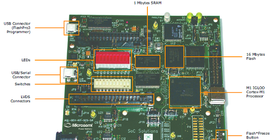
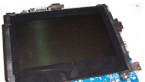
图ProASIC3L开发板M1A3PL-DEV-KIT外形图
ProASIC3L开发板M1A3PL-DEV-KIT主要特性:
• Ultra-low power in Flash*Freeze mode
• Low-power active capability
• Small footprint packages
• Reprogrammable flash technology
• 1.2 V or 1.5 V operation
• High capacity, advanced I/O
• Clock conditioning circuit (CCC) and PLL
• Embedded SRAM and nonvolatile memory (NVM)
• In-system programming (ISP) and security
• Cortex-M1 processor
The Cortex-M1–Enabled IGLOO Development Kit includes the following:
• M1AGL Development Board
• +5.0 V external power supply with international adapters
• 2 USB A to Mini-B cables
• 4 self-adhesive rubber pads
• Quickstart Guide
ProASIC3L开发板M1A3PL-DEV-KIT应用:
The Cortex-M1–Enabled IGLOO Development Kit is ideal for use in the following applications:
• Smartphones, GPS, DCAM, and PDA
• Portable industrial and medical equipment
• PC laptops and PCMCIA
• Any ultra-low power devices
The Cortex-M1–Enabled IGLOO development board has these features:
• Microsemi M1AGL1000 IGLOO FPGA
• 1 MByte SRAM
• 16 MByte flash
• USB–RS232 converter chip
• GPIO connectors
• Ultra-low power with Flash*Freeze technology
• On-board FlashPro3 circuitry
• 20-Pin Cortex-M1 JTAG connector
• Socketed crystal oscillator
• Push-button power-on reset circuit
• 10 test LEDs
• 10 test switches
• Expansion connectors
详情请见:
责任编辑:HanFeng
【免责声明】
1、本文内容、数据、图表等来源于网络引用或其他公开资料,版权归属原作者、原发表出处。若版权所有方对本文的引用持有异议,请联系拍明芯城(marketing@iczoom.com),本方将及时处理。
2、本文的引用仅供读者交流学习使用,不涉及商业目的。
3、本文内容仅代表作者观点,拍明芯城不对内容的准确性、可靠性或完整性提供明示或暗示的保证。读者阅读本文后做出的决定或行为,是基于自主意愿和独立判断做出的,请读者明确相关结果。
4、如需转载本方拥有版权的文章,请联系拍明芯城(marketing@iczoom.com)注明“转载原因”。未经允许私自转载拍明芯城将保留追究其法律责任的权利。
拍明芯城拥有对此声明的最终解释权。


 产品分类
产品分类




 2012- 2022 拍明芯城ICZOOM.com 版权所有 客服热线:400-693-8369 (9:00-18:00)


