


 产品分类
产品分类
基于Microchip公司PAC1934四路直流电源和能源监测方案
 136
136
 拍明
拍明
原标题:Microchip PAC1934四路直流电源和能源监测方案
Microchip公司的PAC1934是带累加器的四路直流电源/能源监测器,具有总线电压监视器和电流检测放大器,直接输入到高分辨率ADC,数字电流进行功率计算和能量累加.监测周期从1ms到36个小时或更长.电源测量精度1%,24位累加器计数,2.7-5.5V工作电压,主要用在笔记本和平板电脑,网络设备,汽车电子,云,Linux和服务器计算和工业与Linux应用.本文介绍了PAC1934主要特性,框图,系统框图和功能框图,以及PAC1934评估板ADM00805主要特性,电路图,材料清单和PCB设计图.
The PAC1934 device is a four-channel energy monitor,with bus voltage monitor and current sense amplifiers thatfeed high-resolution ADCs. Digital circuitry performs power calculations and energy accumulation.
This enables energy monitoring with integration periodsfrom 1 ms up to 36 hours or longer. Bus voltage, senseresistor voltage and accumulated proportional power arestored in registers for retrieval by the system master orEmbedded Controller.
The sampling rate and energy integration period can becontrolled over SMBus or I2C. Active channel selection,one-shot measurements and other controls are also configurableby SMBus or I2C.
The PAC1934 uses real time calibration to minimize offsetand gain errors. No input filters are required for this device.
PAC1934主要特性:
• High-Side Current Monitor
- 100 mV full scale range for current sensevoltage,16b resolution default setting
- Selectable bidirectional current sense capability,
–100 mV to +100 mV range, 16-bittwo’s complement (signed) data format
- External sense resistor sets full scale currentrange
- Very low input current simplifies routing
• Wide Bus Voltage Range for Voltage Monitor
- 0V to 32V input common-mode voltage
- 16-bit resolution for voltage measurements,14b are used for power calculations
• Real Time Auto-Calibration of Offset and GainErrors for Voltage and Current, No User AdjustmentRequired
• 1% Power Measurement Accuracy over a WideDynamic Range
• On-Chip Accumulation of 28-bit Power Results forEnergy Measurement
- 48-bit power accumulator register for recordingaccumulated power data
- 24 bit Accumulator Count
- User programmable sampling rates of 8, 64,256 and 1024 samples per second
- 17 minutes of power data accumulation minimumat 1024 S/s
- >36 hours of power data accumulation minimumat 8 S/s
• 2.7V to 5.5V Supply Operation
- Separate VDD I/O pin for digital I/O
- 1.62-5.5V capable SMBus and digital I/O
- SMBus 3.0 and I2C Fast Mode Plus (1Mb/S)
• SMBus Address - 16 Options, set with Resistor
• No Input Filters Required
• ALERT Features that can be Enabled:
- ALERT on accumulator overflow
- ALERT on Conversion Complete
• 2.225 x 2.17 mm WLCSP Package
PAC1934应用:
• Notebook and Tablet Computing
• Networking
• Automotive
• Cloud, Linux and Server Computing
• Industrial
• Linux Applications
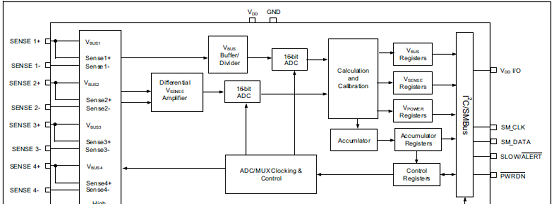
图1.PAC1934框图
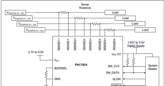
图2.PAC1934系统框图
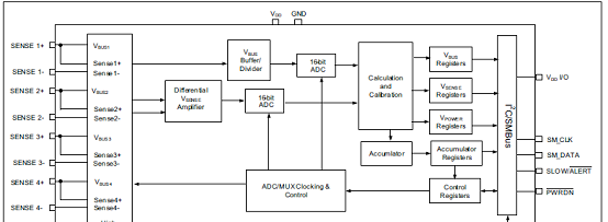
图3.PAC1934功能框图
PAC1934评估板ADM00805
The ADM00805 Evaluation Board for PAC1934 provides a flexible platform for evaluating PAC1934 and demonstrating the features of the PAC1934. A PAC1934 device ina wafer level chip scale package (WLCSP) is mounted to the board.
The ADM00805 has a USB connector to connect to a computer for device communication. The PAC1934 device may be powered directly by VBUS from the USB connectoror by an external connection for VDD.
I2C communication can be provided over USB using the on-board MCP2221 USB toI2C Bridge. There is also a header that facilitates direct I2C communication by connectingthe VDD_IO, Ground, SDA and SCL to an external source such as a PC motherboardor a Linux system.
The shorting shunts and the switch on the board facilitate either simple demonstrationof the device functions using on-board current sources or detailed evaluation offunction and performance with external sources, including prototyping the system.
The ADM00805 Evaluation Board has a PAC1934 device mounted on the board and enables direct control of all device pins and easy measurements of on-board or external voltages and currents. The I2C address is connected as 0x20 by default. Removinga shunt gives 0x22. Other addresses are possible by replacing R22 with a new value.
Sampling rate is 1024 sps by default, due to the shorting shunt on the SLOW pin connector(J23) tying the SLOW pin to ground. Remove this shunt for the SLOW sampling rate of 8 sps.
An on-board current source provides a 0.5 Hz square wave current signal for functionality testing and demo purposes. There are also on-board current sense resistors, provisions for external sources and loads, and provisions for both USB control and directI2C connection.
评估板ADM00805包括:
• The ADM00805 Evaluation Board (EVB)
• USB cable
• Important Information Sheet
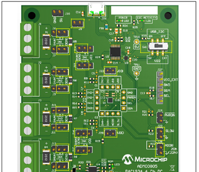
图4.评估板ADM00805外形图
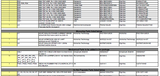
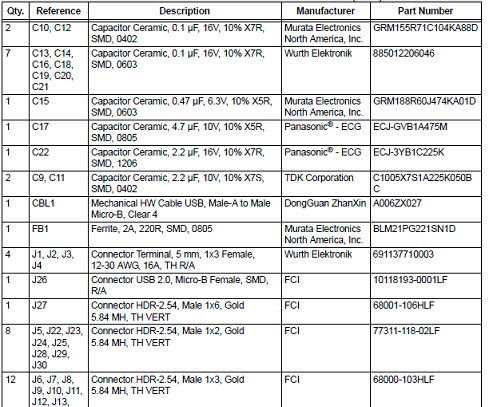
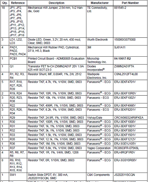
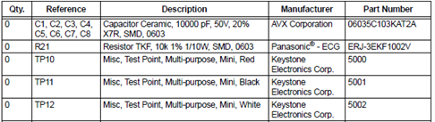
评估板ADM00805材料清单:


详情请见:
责任编辑:Davia
【免责声明】
1、本文内容、数据、图表等来源于网络引用或其他公开资料,版权归属原作者、原发表出处。若版权所有方对本文的引用持有异议,请联系拍明芯城(marketing@iczoom.com),本方将及时处理。
2、本文的引用仅供读者交流学习使用,不涉及商业目的。
3、本文内容仅代表作者观点,拍明芯城不对内容的准确性、可靠性或完整性提供明示或暗示的保证。读者阅读本文后做出的决定或行为,是基于自主意愿和独立判断做出的,请读者明确相关结果。
4、如需转载本方拥有版权的文章,请联系拍明芯城(marketing@iczoom.com)注明“转载原因”。未经允许私自转载拍明芯城将保留追究其法律责任的权利。
拍明芯城拥有对此声明的最终解释权。
相关资讯
:
基于MC33771主控芯片的新能源锂电池管理系统解决方案

AMIC110 32位Sitara ARM MCU开发方案

基于AMIC110多协议可编程工业通信处理器的32位Sitara ARM MCU开发方案

基于展讯SC9820超低成本LTE芯片平台的儿童智能手表解决方案

基于TI公司的AM437x双照相机参考设计

基于MTK6580芯片的W2智能手表解决方案


 2012- 2022 拍明芯城ICZOOM.com 版权所有 客服热线:400-693-8369 (9:00-18:00)


