


 产品分类
产品分类
infineon公司TLE9879汽车三相马达驱动解决方案
 247
247
 拍明芯城
拍明芯城
原标题:infineon公司TLE9879汽车三相马达驱动解决方案
Infineon公司TLE9879汽车三相马达驱动解决方案
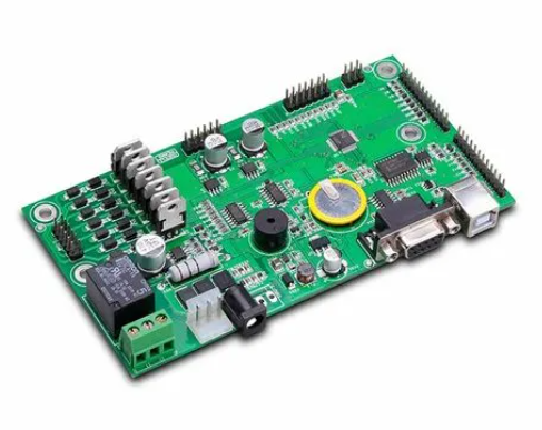
在汽车电子领域,三相无刷直流(BLDC)马达驱动解决方案是提升车辆性能和能效的关键技术之一。Infineon公司的TLE9879系列芯片,特别是TLE9879QXA20,是一款专为汽车级机电一体化BLDC马达驱动应用设计的高度集成解决方案。本文将详细探讨TLE9879QXA20主控芯片的特性、设计中的作用及其在三相马达驱动中的应用。

一、TLE9879QXA20主控芯片概述
TLE9879QXA20是Infineon公司TLE987x产品系列中的一员,是一款集成了ARM Cortex-M3内核的单芯片三相马达驱动器。这款芯片通过集成全面的硬件和软件功能,实现了对BLDC马达的高效控制,广泛应用于燃油泵、HVAC鼓风机、引擎冷却风扇、水泵等汽车关键部件中。
主要特性:
集成ARM Cortex-M3内核:TLE9879QXA20内置了行业标准的32位ARM Cortex-M3微控制器,时钟频率高达24MHz(某些版本如TLE9879QXA40可达40MHz),支持复杂的马达控制算法,如场定向控制(FOC)。
全面的NFET驱动器:芯片包含6个全面集成的NFET驱动器,通过外接功率NFET能够驱动三相马达。这些驱动器具备电荷泵功能,支持低压操作,并可通过编程控制电流和电流斜率,从而优化电磁兼容性(EMC)性能。
丰富的外设接口:TLE9879QXA20集成了多个外设,包括电流传感器、逐次逼近ADC(模拟数字转换器)、16位定时器、LIN收发器等。这些外设支持PWM控制、数据采集、通信等功能,使得芯片能够灵活应对各种控制需求。
宽电源电压范围:支持的工作电源电压范围为5.5V至28V,最高额定电压可达40V。扩展工作电压范围为3.0V至28V,确保在不同电压条件下MCU和闪存均能正常运行。
高ESD性能和过压保护:在所有引脚上具备高达2kV的ESD保护能力,高压输入引脚可达4kV,LIN引脚可达6kV。此外,芯片还具备过压器件箝位功能,能够承受高达40V的负载突降,增强了系统的稳定性和可靠性。
宽工作温度范围:能够在-40℃至150℃的宽温度范围内工作,满足汽车应用的严苛环境要求。
二、TLE9879QXA20在设计中的作用
在汽车三相马达驱动系统中,TLE9879QXA20扮演着核心控制器的角色,通过精确控制马达的转速、扭矩和位置,实现高效、稳定的驱动效果。以下是TLE9879QXA20在设计中的主要作用:
实现高级马达控制算法:
利用集成的ARM Cortex-M3内核,TLE9879QXA20能够运行复杂的马达控制算法,如FOC(场定向控制)。FOC算法通过精确控制马达的磁场方向和电流大小,实现高效、低噪音的马达运行,提升系统整体性能。
精确控制马达运行:
通过集成的电流传感器和ADC模块,TLE9879QXA20能够实时监测马达的电流和电压,确保马达在额定范围内运行。同时,通过PWM控制信号和16位定时器,精确调节马达的转速和扭矩,满足不同应用场景的需求。
优化EMC性能:
TLE9879QXA20的电荷泵功能和可编程电流斜率控制功能,有助于减少电磁干扰(EMI),提升系统的EMC性能。这对于汽车电子系统尤为重要,因为汽车内部存在大量的电磁设备和线路,容易产生相互干扰。
实现通信与数据交换:
集成的LIN收发器使得TLE9879QXA20能够与车辆其他控制单元进行通信,实现数据交换和指令控制。这种通信能力使得马达驱动系统能够与车辆的其他系统(如发动机控制单元、车身控制单元等)协同工作,提升整车的智能化水平。
提供系统保护与安全功能:
TLE9879QXA20具备多种保护机制,包括过压保护、欠压保护、过热保护、短路保护等,确保马达驱动系统在各种异常情况下都能安全运行。同时,集成的可编程窗口看门狗功能能够监测系统运行状态,及时发现并处理潜在问题。
三、TLE9879QXA20在三相马达驱动中的应用
在三相马达驱动系统中,TLE9879QXA20的应用不仅限于基本的控制功能,还深入到系统的优化、故障诊断以及能效提升等多个方面。以下是对其在三相马达驱动中具体应用的进一步阐述:
四、TLE9879QXA20在三相马达驱动中的深入应用
能效优化:
TLE9879QXA20通过精确控制马达的电流和电压,实现了能效的最大化。其内置的FOC算法能够确保电流与磁场方向的最佳匹配,减少能量损失,提高马达的转换效率。此外,通过动态调整PWM信号的占空比,可以进一步优化马达在不同负载条件下的能效表现。
故障诊断与预测性维护:
利用TLE9879QXA20的丰富外设和强大的数据处理能力,可以实现对马达驱动系统的实时监测和故障诊断。通过监测电流、电压、温度等关键参数,系统能够及时发现潜在的故障迹象,如过载、短路、过热等,并采取相应的保护措施。此外,通过数据分析,还可以预测马达的寿命和维护周期,实现预测性维护,减少非计划停机时间。
静音运行:
在汽车应用中,马达的噪音水平是一个重要的考量因素。TLE9879QXA20通过精确控制马达的电流波形和换相过程,可以减少机械振动和电磁噪音,实现马达的静音运行。这对于提升乘客的舒适性和车辆的NVH(噪音、振动和刺耳声)性能具有重要意义。
灵活的配置与扩展性:
TLE9879QXA20提供了丰富的配置选项和扩展接口,使得它能够满足不同应用场景的需求。通过编程和配置,用户可以轻松调整马达的控制参数、通信协议和保护机制等。此外,TLE9879QXA20还支持与其他控制单元和传感器的接口连接,为系统的扩展和升级提供了便利。
安全性与可靠性:
在汽车应用中,安全性和可靠性是至关重要的。TLE9879QXA20通过集成多种保护机制(如过压保护、欠压保护、过热保护等)和强大的故障诊断能力,确保了马达驱动系统的安全运行。同时,其宽工作温度范围和高ESD保护能力也增强了系统的可靠性和耐用性。
五、结论
Infineon公司的TLE9879QXA20是一款专为汽车三相马达驱动设计的高度集成解决方案。通过集成ARM Cortex-M3内核、全面的NFET驱动器、丰富的外设接口以及多种保护机制,TLE9879QXA20实现了对马达的高效、精确控制,并提供了强大的故障诊断和预测性维护功能。在汽车电子领域,TLE9879QXA20的应用不仅提升了马达驱动系统的性能和能效,还增强了系统的安全性和可靠性。随着汽车智能化和电动化趋势的加速发展,TLE9879QXA20等高性能马达驱动解决方案将在未来发挥更加重要的作用。
责任编辑:David
【免责声明】
1、本文内容、数据、图表等来源于网络引用或其他公开资料,版权归属原作者、原发表出处。若版权所有方对本文的引用持有异议,请联系拍明芯城(marketing@iczoom.com),本方将及时处理。
2、本文的引用仅供读者交流学习使用,不涉及商业目的。
3、本文内容仅代表作者观点,拍明芯城不对内容的准确性、可靠性或完整性提供明示或暗示的保证。读者阅读本文后做出的决定或行为,是基于自主意愿和独立判断做出的,请读者明确相关结果。
4、如需转载本方拥有版权的文章,请联系拍明芯城(marketing@iczoom.com)注明“转载原因”。未经允许私自转载拍明芯城将保留追究其法律责任的权利。
拍明芯城拥有对此声明的最终解释权。
相关资讯
:
基于Xilinx XCKU115的半高PCIe x8 硬件加速卡设计方案
图像传感器在汽车、工业和边缘AI的应用动向
基于RFID技术的智能档案管理系统设计方案
如何确保工业物联网设计符合ISA/IEC安全标准
基于LPC55S69+i.MX 8M的快速灵活EV充电系统解决方案
如何利用物质连接智能家居自动化的孤岛


 2012- 2022 拍明芯城ICZOOM.com 版权所有 客服热线:400-693-8369 (9:00-18:00)


