


 产品分类
产品分类
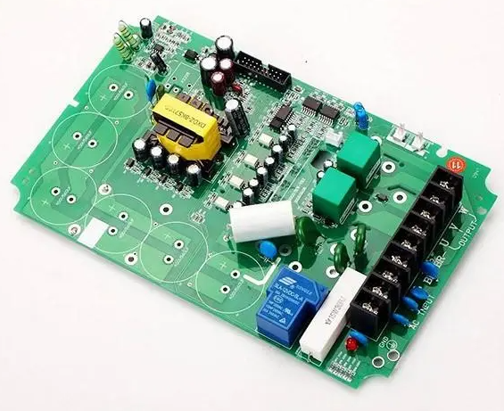
基于Microchip HV9961+PIC16F15313恒流控制LED驱动器解决方案
 127
127
 拍明
拍明
原标题:Microchip HV9961+PIC16F15313恒流控制LED驱动器解决方案
基于Microchip HV9961+PIC16F15313的恒流控制LED驱动器解决方案
恒流控制LED驱动器是一种高效的电路解决方案,广泛应用于照明设备、显示器、背光及其他领域。本文以Microchip HV9961与PIC16F15313为核心,探讨如何设计一套恒流LED驱动器,并详细分析各主控芯片的型号及其作用。

一、方案概述
恒流LED驱动器能够确保LED灯在电流变化较小的条件下工作,从而提高亮度稳定性和使用寿命。设计要求包括高效率、精确的电流控制、热量管理以及对输入电压变化的适应能力。基于Microchip HV9961和PIC16F15313的解决方案是一种经典的组合,结合了高性能的功率转换与灵活的数字控制。
二、核心芯片及其作用
2.1 HV9961恒流控制芯片
HV9961是Microchip公司推出的高性能LED驱动芯片,专为恒流驱动应用设计。其主要特点包括:
支持宽输入电压范围,通常为9V至450V。
提供高精度的电流调节功能。
内置多种保护机制,如短路保护、过压保护和热关断。
在设计中的作用
HV9961的核心任务是通过控制外部MOSFET的开关操作,实现LED灯的恒流驱动。其电流反馈机制能够持续监测负载电流并调节PWM占空比,确保LED电流保持稳定。此外,HV9961内置的降压模式电路使其能够高效处理高压输入电源,并输出适合LED需求的低压恒流。
常见型号
HV9961LG-G: 工作温度范围为-40°C至+125°C,适用于工业和商业领域。
HV9961P: 高效率封装版本,更适合紧凑型设计。
2.2 PIC16F15313单片机
PIC16F15313是一款16位微控制器,具备多功能外设和低功耗特性,适用于LED驱动的数字控制部分。其主要特点包括:
高达8KB的程序存储器和512B的RAM。
多达24个I/O引脚,用于外设控制和信号接口。
内置PWM模块和模数转换器(ADC),支持精确的信号采集和调节。
低功耗设计,适合高效电源管理。
在设计中的作用
PIC16F15313的主要作用是提供灵活的数字控制功能,包括:
处理用户输入或通信命令,调节LED亮度或颜色。
通过ADC采集电流和电压反馈信号,优化恒流控制精度。
实现多种智能功能,如故障检测、调光功能和温度管理。
与HV9961协同工作,生成PWM信号以调节MOSFET开关操作。
常见型号
PIC16F15313-I/SL: 支持工业温度范围的标准型号。
PIC16F15313-E/ML: 高可靠性版本,适合严苛环境。
三、设计实现
3.1 系统框架设计
该LED驱动器设计由三大部分组成:电源管理、恒流控制与数字逻辑控制。HV9961作为恒流控制核心,通过MOSFET调节输出电流,确保LED灯的亮度稳定;PIC16F15313负责实现智能调节功能,包括PWM调光、保护机制及温度管理。
系统框图如下:
输入电源部分:整流与滤波电路,提供稳定的DC电压。
恒流控制部分:HV9961控制外部功率MOSFET的工作状态,实现恒流输出。
数字控制部分:PIC16F15313负责信号采集、PWM调制和通信功能。
3.2 核心电路设计
HV9961恒流控制电路
HV9961需要外接一个电流检测电阻,用于监测输出电流的实时变化。其反馈引脚将检测到的电流信号送入内部比较器,通过调整开关频率来达到恒流控制目标。
PIC16F15313逻辑控制电路
PIC16F15313通过其ADC模块采集HV9961的反馈信号,并根据预设算法调整PWM占空比,从而实现精确控制。此外,PIC16F15313可以通过UART或I2C与上位机通信,实现智能化调节。
3.3 热设计与保护功能
在高功率LED驱动器中,热管理至关重要。HV9961和PIC16F15313均具有内部温度检测功能,能够通过数字控制模块进行动态调节。例如,当检测到温度过高时,PIC16F15313可以降低PWM占空比以减少功耗。
四、实际应用及性能分析
4.1 应用场景
该解决方案适用于多种应用场景,包括:
室内外照明,如路灯、工矿灯和商业照明。
LED显示屏的背光驱动。
高端调光灯具,实现精准亮度和色温控制。
4.2 性能特点
相比传统LED驱动器,该方案具有以下优势:
高效率:HV9961优化的降压电路设计结合PIC16F15313的低功耗控制,使系统效率高达95%以上。
精准调节:通过数字控制器的灵活配置,支持多级调光和色温调整。
强大保护功能:包括过温、短路和过压保护,确保系统安全可靠。
五、扩展功能与未来发展
随着智能照明需求的增加,可以进一步扩展以下功能:
增加无线控制模块,实现远程控制。
使用更高级的PIC单片机,支持多种通信协议(如BLE、Wi-Fi)。
引入AI算法,优化功率分配和灯光调节。
六、结论
基于Microchip HV9961和PIC16F15313的恒流控制LED驱动器是一种高效、灵活和可靠的解决方案。通过合理的芯片选型与电路设计,能够满足多种照明需求,同时为未来的智能化扩展打下基础。这种方案不仅提高了LED灯具的性能,还显著降低了整体功耗,为绿色节能照明贡献力量。
责任编辑:David
【免责声明】
1、本文内容、数据、图表等来源于网络引用或其他公开资料,版权归属原作者、原发表出处。若版权所有方对本文的引用持有异议,请联系拍明芯城(marketing@iczoom.com),本方将及时处理。
2、本文的引用仅供读者交流学习使用,不涉及商业目的。
3、本文内容仅代表作者观点,拍明芯城不对内容的准确性、可靠性或完整性提供明示或暗示的保证。读者阅读本文后做出的决定或行为,是基于自主意愿和独立判断做出的,请读者明确相关结果。
4、如需转载本方拥有版权的文章,请联系拍明芯城(marketing@iczoom.com)注明“转载原因”。未经允许私自转载拍明芯城将保留追究其法律责任的权利。
拍明芯城拥有对此声明的最终解释权。
相关资讯
:
基于Xilinx XCKU115的半高PCIe x8 硬件加速卡设计方案
图像传感器在汽车、工业和边缘AI的应用动向
基于RFID技术的智能档案管理系统设计方案
如何确保工业物联网设计符合ISA/IEC安全标准
基于LPC55S69+i.MX 8M的快速灵活EV充电系统解决方案
如何利用物质连接智能家居自动化的孤岛


 2012- 2022 拍明芯城ICZOOM.com 版权所有 客服热线:400-693-8369 (9:00-18:00)


