基于RZ/A1H、EFR32BG、Si1153支持蓝牙刷卡的通道门(闸机)解决方案
 337
337
 拍明
拍明
概述
通道门(闸机)广泛用于公共场所的出入口,通常通道门支持RFID比较单一的刷卡方式,随着智能手机的广泛普及,刷卡和支付方式多元化,可支持智能手机蓝牙刷卡,二维码扫描,NFC刷卡, Sub-GHz频段遥控开门方式等,让出行和通行更加便利。同时行业上通常采用红外对射的方式检测人员通行状态以及防尾随报警功能,施工时需要考虑红外对管安装位置需要对齐,施工难度大,本方案采用反射式红外检测方式,方便施工安装。
优势
• 采用Cortex A9内核,运行频率高达400MHz的32位MCU(RZ/A1),具有3~10M RAM及24路 12位AD,内置高速 2D 图像加速器,实现高速图像处理(支持 OpenVG1.1),还支持二维码扫描等功能;自带以太网MAC,2个USB接口以及多路IIC/UART/SPI接口,满足闸机众多的通信接口需求。
【RZ/A1H】
RZ/A1H is the premium full-featured part in the RZ/A1 family with an Arm® Cortex®-A9 core running at 400MHz and 10MB of on-chip SRAM to support the largest frame-buffers on-chip.
With 10MB on-chip SRAM, the RZ/A1H supports up to 2 Displays with WXGA (1280x800) resolution without the need for external memory. RZ/A1H enables very compact embedded designs without the need to worry about memory procurement and memory EOL. With RZ/A1H, you can design your embedded system like an MCU and get the performance of a 400MHz Arm® Cortex®-A9 MPU. Enabled for support with Linux, RTOS or Bare-metal, this is the ideal device for designing Intelligent IoT End Point devices with compactness and high performance. Supported in QFP and BGA packages with different sizes to support board layout flexibility and with SDRAM interface to expand up to 128MB of external memory.
Key Features:
| ITEM | RZ/A1H | |
|---|---|---|
Part name/use/ package | 256 pin | R7S721000VLFP |
| Car Accessory | ||
| 256-pinQFP (28mm×28mm) 0.4mm pitch | ||
| R7S721000VCFP | ||
| Industry usage etc. | ||
| 256-pinQFP (28mm×28mm) 0.4mm pitch | ||
| R7S721000VCBG | ||
| Industry usage etc. | ||
| 256-pinBGA (11mm×11mm) 0.5mm pitch | ||
| 324 pin | R7S721001VLBG | |
| Car Accessory | ||
| 324-pinBGA (19mm×19mm) 0.8mm pitch | ||
| R7S721001VCBG | ||
| Industry usage etc. | ||
| 324-pinBGA (19mm×19mm) 0.8mm pitch | ||
Power supply voltage | 3.3V/1.18V | |
Maximum operating frequency | 400MHz | |
CPU core | Arm®Cortex®-A9 (with Jazelle and NEON) | |
On-chip RAM | Large-capacity memory: 10 MB | |
| (For video display/work area; 128 KB are shared with data retention) | ||
Cache memory | Primary cache memory: 64 KB (separated 32K instruction/32K data, TLB128 entry) Secondary cache memory: 128 KB (with CoreLink™ Level 2 Cache Controller L2C-310) | |
| External memory | Bus clock: up to 66.67 MHz | |
| Direct connection to SRAM, byte select SRAM, SDRAM, and burst ROM (clock synchronous/clock asynchronous) using bus state controller. Address/data multiplexer I/O (MPX) interface supported. | ||
Address space: 64 MB × 6 | ||
Data bus width: external 8/16/32 bits | ||
Graphics functions | OpenVG1.1 2D graphics accelerator | |
| Video display controller (2 channels of video input and 2 channels of panel output, of which 1 channel supports LVDS) | ||
| Video decoder × 2 channels (analog composite direct input is possible) | ||
| Distortion correction engine × 2 channels (requires nondisclosure agreement) | ||
| Distortion correction engine for display (requires nondisclosure agreement) | ||
| Display out compare unit | ||
| JPEG codec unit | ||
| Capture engine unit (CMOS camera interface) | ||
| Pixel format converter × 2 channels | ||
Audio functions | SCUX (with built-in asynchronous sampling rate conversion, digital volume & mute, and mixer function) | |
| Serial sound interface × 6 channels | ||
| Renesas SPDIF interface | ||
| Sound generator × 4 channels | ||
| CD-ROM decoder | ||
Timer functions | Multifunction 16-bit timer (MTU2) × 5 channels | |
| 32-bit OS timer × 2 channels | ||
| Motor control PWM timer × 8 channels | ||
| Watchdog timer | ||
| Real-time clock | ||
Connectivity functions | USB 2.0 host/function module × 2 channels (host or functon selectable) | |
| NAND flash interface | ||
| SD host interface × 2 channels (must obtain SD card license) | ||
| MMC host interface | ||
| Ethernet controller (10 Mbps/100 Mbps transfer, IEEE802.3 PHY interface MII) | ||
| Ethernet AVB (IEEE802.1 Audio/Video Bridging) controller (requires nondisclosure agreement) | ||
| SPI multi I/O bus controller × 2 channels (up to 2 serial flash memory connectable to 1 channel, direct execution from CPU supported) | ||
| Serial communication interface with 16-stage FIFO (SCIF) × 8 channels (asynchronous and clock synchronous serial communication possible) | ||
| Serial communication interface × 2 channels (smart card interface, IrDA 1.0) | ||
| Renesas serial peripheral interface × 5 channels | ||
| I2C bus interface × 4 channels | ||
| Media Local Bus (MediaLB Ver2.0) | ||
| Controller area network (CAN) × 5 channels | ||
| Local interconnect network interface (LIN) × 2 channels | ||
System analog functions | Clock pulse generator (CPG): built-in PLL, maximum 32 times multiplication, built-in SSCG circuit | |
| Direct memory access controller × 16 channels | ||
| Interrupt controller (with Arm®Generic Interrupt Controller [PL390]) | ||
| A/D converter (12-bit resolution) × 8 channels | ||
| Debugging interface | ||
| CoreSight™ architecture | ||
| JTAG standard pin layout | ||
Optional function | Encryption engine (requires nondisclosure agreement) | |
| Boot modes | Boot mode 0: Boot from memory connected to CS0 space (16-bit bus) | |
| Boot mode 1: Boots from memory connected to CS0 space (32-bit bus) | ||
| Boot mode 2: (not defined) | ||
| Boot mode 3: Boot from serial flash memory | ||
| Boot mode 4: Boot from built-in NAND flash memory of SD controller | ||
| Boot mode 5: Boot from built-in NAND flash memory of MMC controller | ||
| Power-down modes | Sleep mode | |
| Software standby mode | ||
| Deep standby mode | ||
| Module standby mode | ||
Pin count /Memory size Lineup:
SRAM
| 10240KB | ● | ● | ● |
|---|---|---|---|
| Pins Package | 256 LFQFP | 256 LFBGA | 324 FBGA |
Block Diagram:
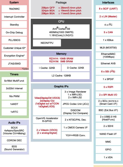
RZ/A1H Block Diagram
*Arm, Cortex, CoreLink, and CoreSight are registered trademarks or trademarks of Arm Limited.
OpenVG is a trademark of the Khronos Group.
CAN (Controller Area Network): An automotive network specification developed by Robert Bosch GmbH of Germany.
LIN (Local Interconnect Network): An automotive network specification established by the LIN Consortium.
MediaLB (Media Local Bus): A registered trademark of SMSC, and an automotive network specification developed by SMSC.
IEBus™ (Inter Equipment Bus) is a trademark of Renesas Electronics Corporation.
All other names of products or services mentioned here are trademarks or registered trademarks of their respective owners.
• 低功耗智能蓝牙SOC(EFR32BG),支持蓝牙5.0版本,是蓝牙4.x版本2倍的速度,4倍的距离及8倍的广播能力,可用于支持闸机手机蓝牙刷卡功能。
【EFR32BG】
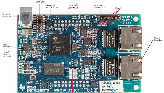
EFR32BG 2.4 GHz 10.5 dBm Radio Board BRD4100A Reference Manual
The EFR32BG family of Wireless SoCs deliver a high performance,low energy wireless solution integrated into a small form factor package.
By combining a high performance 2.4 GHz RF transceiver with an energy efficient 32-bitMCU, the family provides designers the ultimate in flexibility with a family of pin-compatibledevices that scale from 128/256 kB of flash and 16/32 kB of RAM. The ultra-lowpower operating modes and fast wake-up times of the Silicon Labs energy friendly 32-bit MCUs, combined with the low transmit and receive power consumption of the 2.4 GHz radio, result in a solution optimized for battery powered applications.
To develop and/or evaluate the EFR32 Blue Gecko, the EFR32BG Radio Board can beconnected to the Wireless Starter Kit Mainboard to get access to display, buttons andadditional features from Expansion Boards.

RADIO BOARD FEATURES
• Wireless SoC:EFR32BG1P232F256GM48
• CPU core: ARM Cortex-M4 with FPU
• Flash memory: 256 kB
• RAM: 32 kB
• Operation frequency: 2.4 GHz
• Transmit power: 10.5 dBm
• Integrated PCB antenna, UFL connector(optional).
• Crystals for LFXO and HFXO: 32.768 kHz and 38.4 MHz.
1. Introduction
The EFR32 Blue Gecko Radio Boards provide a development platform (together with the Wireless Starter Kit Mainboard) for the SiliconLabs EFR32 Blue Gecko Wireless System on Chips and serve as reference designs for the matching network of the RF interface.
The BRD4100A Radio Board is designed to operate in the 2400-2483.5 MHz band with the RF matching network optimized to operatewith 10.5 dBm output power.
To develop and/or evaluate the EFR32 Blue Gecko, the BRD4100A Radio Board can be connected to the Wireless Starter Kit Mainboard to get access to display, buttons and additional features from Expansion Boards and also to evaluate the performance of the RFinterface.
2. Radio Board Connector
2.1 Introduction
The board-to-board connector scheme allows access to all EFR32BG1 GPIO pins as well as the RESETn signal. For more information on the functions of the available pin functions, see the EFR32BG1 data sheet.
2.2 Radio Board Connector Pin Associations
The figure below shows the pin mapping on the connector to the radio pins and their function on the Wireless Starter Kit Mainboard.
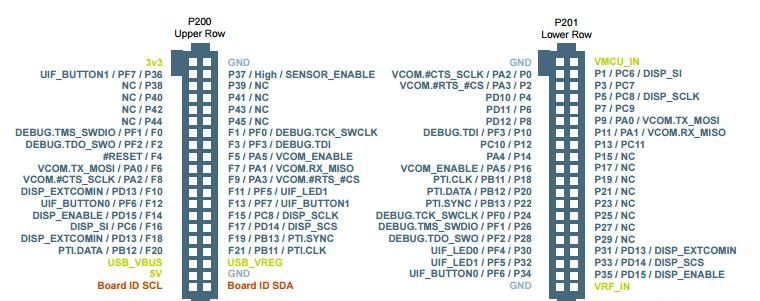
3. Radio Board Block Summary
3.1 Introduction
This section gives a short introduction to the blocks of the BRD4100A Radio Board.
3.2 Radio Board Block Diagram
The block diagram of the EFR32BG Radio Board is shown in the figure below.
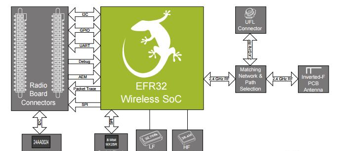
3.3 Radio Board Block Description
3.3.1 Wireless MCU
The BRD4100A EFR32 Blue Gecko Radio Board incorporates an EFR32BG1P232F256GM48 Wireless System on Chip featuring 32-bitCortex-M4 with FPU core, 256 kB of flash memory and 32 kB of RAM and a 2.4 GHz band transceiver with output power up to 10.5dBm. For additional information on the EFR32BG1P232F256GM48, refer to the EFR32BG1 Data Sheet.
3.3.2 LF Crystal Oscillator (LFXO)
The BRD4100A Radio Board has a 32.768 kHz crystal mounted.
3.3.3 HF Crystal Oscillator (HFXO)
The BRD4100A Radio Board has a 38.4 MHz crystal mounted.
3.3.4 Matching Network for 2.4 GHz
The BRD4100A Radio Board incorporates a 2.4 GHz matching network which connects the 2.4 GHz TRX pin of the EFR32BG1 to theone on-board printed Inverted-F antenna. The component values were optimized for the 2.4 GHz band RF performace and current consumptionwith 10.5 dBm output power.For detailed description of the matching network, see Chapter 4.2.1 Description of the 2.4 GHz RF Matching.
3.3.5 Inverted-F Antenna
The BRD4100A Radio Board includes a printed Inverted-F antenna (IFA) tuned to have close to 50 Ohm impedance at the 2.4 GHz
band.
For detailed description of the antenna see Chapter 4.5 Inverted-F Antenna.
3.3.6 UFL Connector
To be able to perform conducted measurements, Silicon Labs added an UFL connector to the Radio Board. The connector allows an external 50 Ohm cable or antenna to be connected during design verification or testing.
Note: By default the output of the matching network is connected to the printed Inverted-F antenna by a series component. It can be connected to the UFL connector as well through a series 0 Ohm resistor which is not mounted by default. For conducted measurements through the UFL connector the series component to the antenna should be removed and the 0 Ohm resistor should be mounted (see Chapter 4.2 Schematic of the RF Matching Network for further details).
3.3.7 Radio Board Connectors
Two dual-row, 0.05” pitch polarized connectors make up the EFR32BG Radio
Board interface to the Wireless Starter Kit Mainboard. For more information on
the pin mapping between the EFR32BG1P232F256GM48 and the Radio Board Connector,
refer to Chapter 2.2 Radio Board Connector Pin Associations.
• 反射式红外检测传感器(Si1153),内部集成3路LED驱动,支持阳光直射的各种光源下工作且其探测距离可从 1cm调节到超过 2米,反射式红外检测方式方便设备安装。
【Si1153】
Proximity/Ambient Light Sensor IC with I2C Interface
The Si1153-AA00/AA09/AA9x is an ambient light sensor, proximity, and gesture detectorwith I2C digital interface and programmable-event interrupt output.
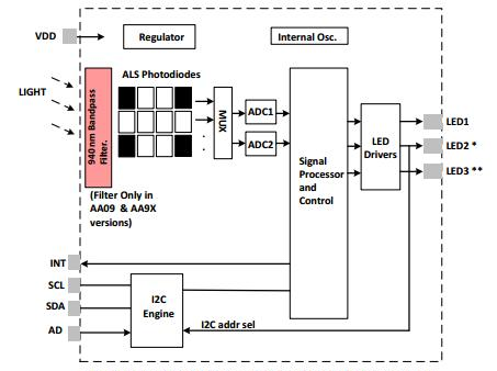
This touchless sensor IC includes dual 23-bit analog-to-digital converters, an integratedhigh-sensitivity array of visible and infrared photodiodes, a digital signal processor, andthree integrated LED drivers with programmable drive levels. The Si1153 offers excellentperformance under a wide dynamic range and a variety of light sources, includingdirect sunlight. The Si1153 can also work under dark glass covers. The photodiode responseand associated digital conversion circuitry provide excellent immunity to artificiallight flicker noise and natural light flutter noise. With two or more LEDs, the Si1153 iscapable of supporting multiple-axis proximity motion detection. The Si1153 is provided ina 10-lead 2x2 mm DFN package or in a 10-lead 2.9x4.9 mm LGA module with integratedLED, and is capable of operation from 1.62 to 3.6 V over the –40 to +85 °C temperaturerange.
KEY FEATURES
• Proximity detector
• From under 1 cm, to 50 cm withoutadditional lensing.
• From under 1 cm, to 200 cm with additional lensing (e.g., 5 mm hemispherical lens as in our EVB).
• Up to three independent LED drivers.
• 30 current settings from 5.6 mA to 360mA for each LED driver.
• Operates in direct sunlight with optionalon-die 940 nm passband filter.
• On die 940 bandpass filter that rejectsunwanted visible light and IR fromdaylight and other sources (Si1153-AA09/AA9X).
• Ambient light sensor
• <100 mlx resolution possible, allowingoperation under dark glass.
• Up to 128 klx dynamic range possibleacross two ADC range settings.
• Industry’s lowest power consumption
• 1.62 to 3.6 V supply voltage.
• 9 μA average current (LED pulsed 25.6μs every 800 ms at 180 mA plus 3 μASi1153 supply).
• <500 nA standby current.
• 25.6 μs LED “on” time keeps total powerconsumption duty cycle low withoutcompromising performance or noisecommunity.
• Internal and external wake support.
• Built-in voltage supply monitor andpower-on reset controller.
APPLICATIONS
• Wearables
• Handsets
• Display backlighting control
• Consumer electronics
1. Feature List
• Proximity detector
• From under 1 cm to 50 cm without additional lensing.
• From under 1 cm to 200 cm with additional lensing (e.g., 5mm hemispherical lens).
• Up to three independent LED drivers.
• 30 current settings from 5.6 mA to 360 mA for each LEDdriver.
• Operates in direct sunlight with optional on-die 940 nmpassband filter.
• On die 940 bandpass filter that rejects unwanted visible lightand IR from daylight and other sources (Si1153- AA09/AA9X).
• Ambient light sensor
• <100 mlx resolution possible, allowing operation under darkglass.
• Up to 128 klx dynamic range possible across two ADCrange settings.
• Industry’s lowest power consumption
• 1.62 to 3.6 V supply voltage.
• 9 μA average current (LED pulsed 25.6 μs every 800 ms at180 mA plus 3 μA Si1153 supply).
• <500 nA standby current.
• 25.6 μs LED “on” time keeps total power consumption dutycycle low without compromising performance or noise community.
• Internal and external wake support.
• Built-in voltage supply monitor and power-on reset controller.
• Trim-able internal oscillator with typical 1% accuracy.
• I2C Serial communications
• Up to 3.4 Mbps data rate.
• Slave mode hardware address decoding.
• Two package options:
• 10-lead 2 x 2 x 0.65 mm DFN
• 10-lead 2.9 x 4.9 x1.2 mm LGA module with integrated 940nm LED
• Temperature Range: –40 to +85 °C
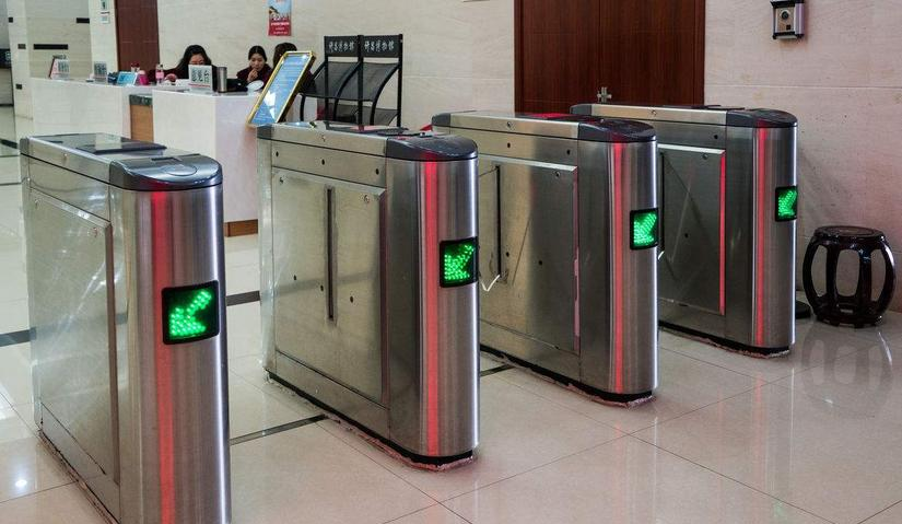
【闸机】
闸机,是一种通道阻挡装置(通道管理设备),用于管理人流并规范行人出入,主要应用于地铁闸机系统、收费检票闸机系统。其最基本最核心的功能是实现一次只通过一人,可用于各种收费、门禁场合的入口通道处。
中国最早应用闸机是80年代期间,用于地铁项目中。闸机作为“自动售检票系统AFC”中的“自动检票机”的主要设备,也是目前国人对闸机最早和最广泛的理解。90年代后期,闸机才渐渐出现在普通民用和商用场合,包括写字楼、商场超市、景区乃至高端小区等。
需要指出的是,闸机和检票机不是完全相同的概念。检票机包括自动检票机和便携式检票机,自动检票机是闸机结合票务系统的一种具体应用。闸机的范围更广,只要是用于管理人流出入且能满足一次只通行一人的设备都可以视为广义的闸机。
闸机的应用场合分室内外,室内外环境不一样,适用的闸机也不一样。
室内所有种类的闸机均适用。
室外使用是完全露天或有遮挡物,但都需考虑日晒、雨淋、沙尘、超高温、超低温、昼夜温差大等户外恶劣环境,室外闸机需要能抵挡这些 天气问题,适用的闸机包括专门针对室外使用设计的户外摆闸、户外翼闸、半自动三辊闸、半自动全高转闸。
户外闸机基本需求:防水防尘等级IP65、耐高温、耐低温、抗阳光干扰,户外摆闸、户外翼闸、半自动三辊闸、半自动全高转闸通过特殊定制都能实现。
户外闸机高级需求:人车共用、抗暴力撞闸。在某些场合,行人可能骑自行车、推婴儿车、坐轮椅等,户外翼闸、半自动三辊闸、半自动全高转闸这三者不能满足这个需求,人车共用户外摆闸可以满足,另外闸机会有被自行车撞击的现象,需具备抗暴力撞闸功能。
责任编辑:Davia
【免责声明】
1、本文内容、数据、图表等来源于网络引用或其他公开资料,版权归属原作者、原发表出处。若版权所有方对本文的引用持有异议,请联系拍明芯城(marketing@iczoom.com),本方将及时处理。
2、本文的引用仅供读者交流学习使用,不涉及商业目的。
3、本文内容仅代表作者观点,拍明芯城不对内容的准确性、可靠性或完整性提供明示或暗示的保证。读者阅读本文后做出的决定或行为,是基于自主意愿和独立判断做出的,请读者明确相关结果。
4、如需转载本方拥有版权的文章,请联系拍明芯城(marketing@iczoom.com)注明“转载原因”。未经允许私自转载拍明芯城将保留追究其法律责任的权利。
拍明芯城拥有对此声明的最终解释权。


 产品分类
产品分类




 2012- 2022 拍明芯城ICZOOM.com 版权所有 客服热线:400-693-8369 (9:00-18:00)


