Lattice CrossLink-NX低功耗FPGA嵌入可视和AI应用方案
 110
110
 拍明
拍明
原标题:Lattice CrossLink-NX低功耗FPGA嵌入可视和AI应用方案
lattice公司的CrossLink-NX系列是低功耗FPGA,支持各种多种高带宽传感器和显示器接口,视频处理和机器学习推理.采用Lattice公司的Nexus FPGA平台,低功耗28nm FD-SOI技术,组合了极为灵活的FPGA和低功耗以及FD-SOI技术的高可靠性(由于极低SER),提供小占位面积的封装选择. CrossLink-NX系列支持各种接口包括MIPI D-PHY (CSI-2, DSI), LVDS, SLVS, subLVDS, PCI Express (Gen1, Gen2), SGMII(吉比特以太网)等.处理特性包括高达39K逻辑单元,56个18x18乘法器,2.9Mb嵌入存储器(包括EBR和LRAM区块),分布式存储器,DRAM接口(支持DDR3,DDR3L,LPDDR2,LPDDR3高达1066Mbpsx16数据宽度),以及用于软处理器的ALU组成部分.CrossLink-NX系列FPGA支持可配置基于SRAM逻辑架构快速配置,可编sysI/O™ 和TransFR™现场升级特性的超快速配置(不到3ms).安全特性包括比特流加密和密码保护.除了FD-SOI技术固有的高可靠性, 主动可靠性特性还包括内置基于帧的SED/SEC(用于基于SRAM的逻辑架构)和ECC(用于EBR和LRAM),每个器件还内置了ADC,用于系统监视特性.主要用在通信,计算,工业,汽车和消费电子系统的创新嵌入式视觉和AI解决方案.本文介绍了CrossLink-NX FPGA主要特性, CrossLink-NX-40 FPGA简化框图和CrossLink-NX-17 FPGA简化框图与时钟图, 以及CrossLink™-NX评估板主要特性,框图,电路图,材料清单和PCB设计图.
CrossLink™-NX family of low-power FPGAs can be used in a wide range of applications, and are optimized for bridging and processing needs in Embedded Vision applications – supporting a variety of high bandwidth sensor and display interfaces, video processing and machine learning inferencing. It is built on Lattice Nexus FPGA platform, using low-power 28 nm FD-SOI technology. It combines the extreme flexibility of an FPGA with the low power and high reliability (due to extremely low SER) of FD-SOI technology, and offers small footprint package options.
CrossLink-NX supports a variety of interfaces including MIPI D-PHY (CSI-2, DSI), LVDS, SLVS, subLVDS, PCI Express (Gen1, Gen2), SGMII (Gigabit Ethernet), and more.
Processing features of CrossLink-NX include up to 39K Logic Cells, 56 18x18 multipliers, 2.9 Mb of embedded memory (consisting of EBR and LRAM blocks), distributed memory, DRAM interfaces (supporting DDR3, DDR3L, LPDDR2, LPDDR3 up to 1066 Mbps x 16 data width), and ALU building blocks for soft processor.
CrossLink-NX FPGAs support fast configuration of its reconfigurable SRAM-based logic fabric, ultra-fast configuration (in under 3 ms) of its programmable sysI/O™ and TransFR™ field upgrade feature. Security features to secure user designs include bitstream encryption and password protection. In addition to the high reliability inherent to FD-SOI technology (due to its extremely low SER), active reliability features such as built-in frame-based SED/SEC (for SRAM-based logic fabric), and ECC (for EBR and LRAM) are also supported. Built-in ADC is available in each device for system monitoring functions.
Lattice Radiant® design software allows large complex user designs to be efficiently implemented on CrossLink-NX FPGA family. Synthesis library support for CrossLink-NX devices is available for popular logic synthesis tools. Radiant tools use the synthesis tool output along with constraints from its floor planning tools, to place and route the user design in CrossLink-NX device. The tools extract timing from the routing, and back-annotate it into the design for timing verification.
Lattice provides many pre-engineered IP (Intellectual Property) modules for CrossLink-NX family. By using these configurable soft IP cores as standardized blocks, you are free to concentrate on the unique aspects of your design, increasing your productivity.
CrossLink-NX FPGA主要特性:
· Programmable Architecture
· 17K to 39K logic cells
· 24 to 56 18 x 18 multipliers (in sysDSP™ blocks)
· 2.5 to 2.9 Mb of embedded memory blocks (EBR, LRAM)
· 36 to 192 programmable sysI/O (High Performance and Wide Range I/O)
· MIPI D-PHY
· Up to two hardened 4-lane MIPI D-PHY interfaces
· Up to 8 lanes total
· Transmit or receive
· Supports CSI-2, DSI
· 20 Gbps aggregate bandwidth
· 2.5Gbps per lane, 10 Gbps per D-PHY interface
· Additional Soft D-PHY interfaces supported by High Performance (HP) sysI/O
· Transmit or receive
· Supports CSI-2, DSI
· Up to 1.5 Gbps per lane
· Programmable sysI/O supports wide variety of interfaces
· High Performance (HP) on bottom I/O dual rank
· Supports up to 1.8 V VCCIO
· Mixed voltage support (1.0 V, 1.2 V, 1.5 V, 1.8 V)
· High-speed differential up to 1.5 Gbps
· Supports soft D-PHY (Tx/Rx), LVDS 7:1 (Tx/Rx), SLVS (Tx/Rx), subLVDS (Rx)
· Supports SGMII (Gb Ethernet) – 2 channels (Tx/Rx) at 1.25 Gbps
· Dedicated DDR3/DDR3L and LPDDR2/LPDDR3 memory support with DQS logic, up to 1066 Mbps data-rate and x16 data-width
· Wide Range (WR) on Left, Right and Top I/O Banks
· Supports up to 3.3 V VCCIO
· Mixed voltage support (1.2 V, 1.5 V, 1.8 V, 2.5 V, 3.3 V)
· Programmable slew rate (slow, med, fast)
· Controlled impedance mode
· Emulated LVDS support
· Hot-socketing
· Power Modes – Low Power versus High-Performance
· User selectable
· Low-Power mode for power and/or thermal challenges
· High-Performance mode for faster processing
· Small footprint package options
· 4 x 4 mm2 to 10 x 10 mm2 package options
· 2x SGMII CDR at up to 1.25 Gbps – to support 2 channels SGMII using HP I/O
· CDR for RX
· 8b/10b decoding
· Independent Loss of Lock (LOL) detector for each CDR block
· sysCLOCK™ analog PLLs
· Three in 39K LC and two in 17K LC device
· Six outputs per PLL
· Fractional N
· Programmable and dynamic phase control
· sysDSP Enhanced DSP blocks
· Hardened pre-adder
· Dynamic Shift for AI/ML support
· Four 18 x 18, eight 9 x 9, two 18 x 36, or 36 x 36
· Advanced 18 x 36, two 18 x 18, or four 8 x 8 MAC
· Flexible memory resources
· Up to 1.5 Mb sysMEM™ Embedded Block RAM (EBR)
· Programmable width
· ECC
· FIFO
· 80k to 240k bits distributed RAM
· Large RAM Blocks
· 0.5 Mbits per block
· Up to five blocks (2.5 Mb total) per device
· ALU Features
· RISC-V compliant ALU
· Register file
· SERDES – PCIe Gen2 x1 channel (Tx/Rx) hard IP in 39K LC device
· Hard IP supports
· Gen1, Gen2, Multi-Function, End Point, Root Complex
· APB control bus
· AHB-Lite for data bus
· Internal bus interface support
· APB control bus
· AHB-Lite for data bus
· AXI4-streaming
· Configuration – Fast, Secure
· SPI – x1, x2, x4 up to 150 MHz
· Master and Slave SPI support
· JTAG
· I2C and I3C
· Ultrafast I/O configuration for instant-on support
· Less than 15 ms full device configuration for LIFCL-40
· Bitstream Security
· Encryption
· Single Event Upset (SEU) Mitigation Support
· Extremely low Soft Error Rate (SER) due to FD-SOI technology
· Soft Error Detect – Embedded hard macro
· Soft Error Correction – Without stopping user operation
· Soft Error Injection – Emulate SEU event to debug system error handling
· ADC – 1 MSPS, 12-bit SAR
· 2 ADCs per device
· 3 Continuous-time Comparators
· Simultaneous sampling
· System Level Support
· IEEE 1149.1 and IEEE 1532 compliant
· Reveal Logic Analyzer
· On-chip oscillator for initialization and general use
· 1.0 V core power supply
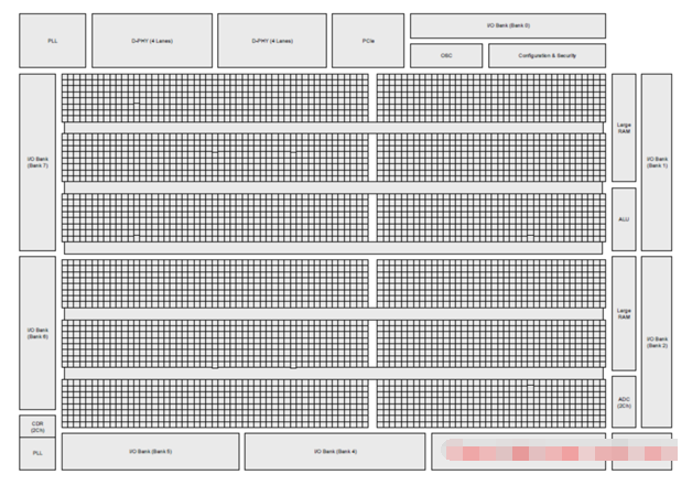
图1. CrossLink-NX-40 FPGA简化框图
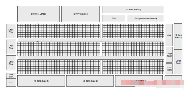
图2. CrossLink-NX-17 FPGA简化框图
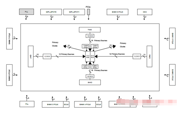
图3. CrossLink-NX FPGA时钟框图
CrossLink™-NX评估板
CrossLink-NX Evaluation Board
The Lattice Semiconductor CrossLink™-NX Evaluation Board allows designers to investigate and experiment with the features of the CrossLink-NX Field Programmable Gate Array (FPGA). The features of the CrossLink-NX Evaluation Board can assist engineers with the rapid prototyping and testing of their specific designs.
The CrossLink-NX Evaluation Board is part of the CrossLink-NX Evaluation Kit, which includes the following:
· CrossLink-NX Evaluation Board pre-loaded with the shipping demo design
· 12 V AC/DC power adapter and international plug adapters
· Lattice Radiant® Software license information
· USB-A to USB-B (Mini) Cable for programming FPGA through a PC
· Quick Start Guide
The contents of this user guide include top-level functional descriptions of the various portions of the development board, descriptions of the on-board headers, diodes and switches and a complete set of schematics.
The CrossLink-NX Evaluation Board features the CrossLink-NX FPGA in the 400-ball caBGA package (LIFCL-40-9BG400C) w the ability to expand the usability of the CrossLink-NX with Raspberry Pi, PMOD, FMC LPC connector, along with access to PCIe channel. 118 wide range I/O and 37 high speed differential pairs are available for user-defined applications.
CrossLink™-NX评估板主要特性:
The CrossLink-NX Evaluation Board includes the following features:
· CrossLink-NX FPGA (LIFCL-40-9BG400C)
· General Purpose Input/Output (GPIO) breakout with Raspberry Pi, PMOD, and FMC connector
· MIPI CSI-2 Camera connector and D-PHY connector
· 118 wide range I/O and 37 high speed differential pair I/O with on board termination
· x1 Gen2 PCIe interface
· USB-B connection for device programming and Inter-Integrated Circuit (I2C) utility
· On-board Boot Flash – 128 Mbit Serial Peripheral Interface (SPI) Flash, with Quad read feature
· Eight input DIP switches, four push buttons, three status LEDs and 14 LEDs for demo purposes
· Lattice Radiant® Software programming support
· Multiple reference clock sources
· Potentiometer for ADC test
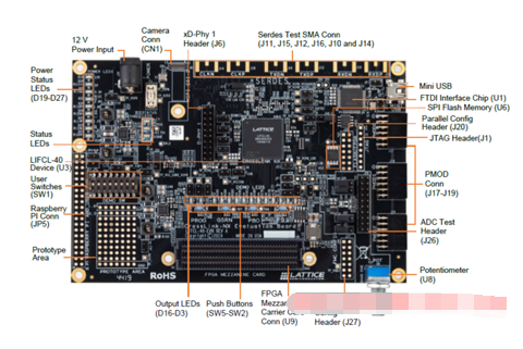
图4. CrossLink™-NX评估板外形图(正面)
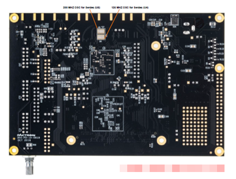
图5. CrossLink™-NX评估板外形图(背面)
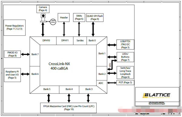
图6. CrossLink™-NX评估板框图
责任编辑:David
【免责声明】
1、本文内容、数据、图表等来源于网络引用或其他公开资料,版权归属原作者、原发表出处。若版权所有方对本文的引用持有异议,请联系拍明芯城(marketing@iczoom.com),本方将及时处理。
2、本文的引用仅供读者交流学习使用,不涉及商业目的。
3、本文内容仅代表作者观点,拍明芯城不对内容的准确性、可靠性或完整性提供明示或暗示的保证。读者阅读本文后做出的决定或行为,是基于自主意愿和独立判断做出的,请读者明确相关结果。
4、如需转载本方拥有版权的文章,请联系拍明芯城(marketing@iczoom.com)注明“转载原因”。未经允许私自转载拍明芯城将保留追究其法律责任的权利。
拍明芯城拥有对此声明的最终解释权。


 产品分类
产品分类




 2012- 2022 拍明芯城ICZOOM.com 版权所有 客服热线:400-693-8369 (9:00-18:00)


