Microchip MCP16501 SAMA5DX系列MPU最佳PMIC解决方案
 126
126
 拍明
拍明
原标题:Microchip MCP16501 SAMA5DX系列MPU最佳PMIC解决方案
microchip公司的MCP16501是用于SAMA5DX/SAM9X6/SAMA7G系列MPU的成本和尺寸最佳的电源管理集成电路(PMIC),和Microchip公司的嵌入微处理器单元(EMPU)以及相关的DRAM存储器兼容.所有的降压通路负载电流高达1A,100%占空比.300mA LDO支持敏感的模拟负载.而DDR存储器电压(Buck2输出)和MPU核电压(Buck3输出)由两个3态输入引脚来选择.这种方法在输出电压设定时有更好的精度(±1%),因为不需要外接反馈电阻,同时还减少外接元件.输入电压2.7V-5,5V,降压通路2MHz PWM操作,引脚选择Buck2:输出电压: 1.2V, 1.35V, 1.8V; Buck3输出电压: 1.0V, 1.15V和1.25V.工作温度-40C到 +125C,采用24引脚4 mm x 4 mm VQFN封装.低功耗模式静态电流250 μA,最大关断电流为 6 μA .主要用在高性能MPU电源解决方案和μC/μP, FPGA以及DSP电源.本文介绍了MCP16501主要特性,框图,典型应用电路和评估板MIC28516主要特性,电路描述图和电路图,材料清单和PCB设计图.
The MCP16501 is a cost and size optimized integrated PMIC, compatible with Microchip s EMPUs (Embedded Microprocessor Units) and associated DRAM Memories.
It is compatible with SAMA5DX, SAM9X6 and SAMA7G MPUs, which are supported by dedicated device variants.
The MCP16501 integrates three DC-DC Buck regulators and one auxiliary LDO, and provides a comprehensive interface to the MPU.
All Buck channels can support loads up to 1A and are 100% duty cycle-capable.
The 300 mA LDO is provided such that sensitive analog loads can be supported.
The DDR memory voltage (Buck2 output) and MPU core voltage (Buck3 output) are selectable by means of two 3-state input pins. This method allows greater precision in the output voltage setting by eliminating inaccuracies due to external feedback resistors, while
minimizing external component count. The voltage selection set allows easy migration across different generations of memory.
The default power channel sequencing is built-in according to the requirements of the MPU. A dedicated pin (LPM) facilitates the transition to Low-Power modes and the implementation of Backup mode with DDR in self-refresh (Hibernate mode).
The MCP16501 features a low no-load operational quiescent current and it draws less than 6 μA (VIN =4.5V, TJ = +105C) in full shutdown.
Active discharge resistors are provided on each output.
All Buck channels support safe start-up into pre-biased outputs.
The MCP16501 is available in a 24-pin 4 mm x 4 mm VQFN package with an operating junction temperature range from -40C to +125C.
MCP16501主要特性:
• Input Voltage: 2.7V to 5.5V
• Three 1A Output Current Buck Channels with 100% Maximum Duty Cycle Capability
• 2 MHz Buck Channels PWM Operation
• One Auxiliary 300 mA Low-Dropout Linear Regulator (LDO)
• ±1% Voltage Accuracy for DDR (Buck2 Output) and Core (Buck3 Output)
• Pin-Selectable Output Voltages for Buck2:
1.2V, 1.35V, 1.8V and for Buck3: 1.0V, 1.15V, 1.25V
• MPU-Specific Built-in Default Channel Sequencing and nRSTO Assertion Delay
• Support of MPU Hibernate, Low-Power Modes
• Low Noise, Forced PWM (FPWM) and Low IQ, Light Load, High-Efficiency Mode Available
• Leakage-Free Interfacing to MPU in any Operating Condition through Optimized ESD Protection
• 250 μA Low-Power Mode Typical Quiescent Current Bucks and LDO On, No Load
• 6 μA Maximum Shutdown Current (VIN = 4.5V, TJ = +105C)
• Separate LDO EN Input, Compatible to LV Logic
• Cost and Size-Optimized BOM
• Thermal Shutdown and Current Limit Protection
• 24-Pin 4 mm × 4 mm VQFN Package
• -40C to +125C Junction Temperature Range
MCP16501应用:
• High-Performance MPUs Power Supply Solutions
• μC/μP, FPGA and DSP Power
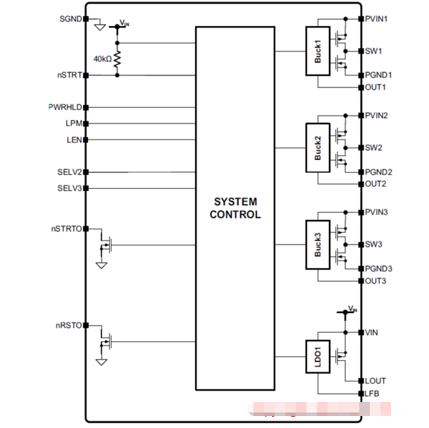
图1. MCP16501框图
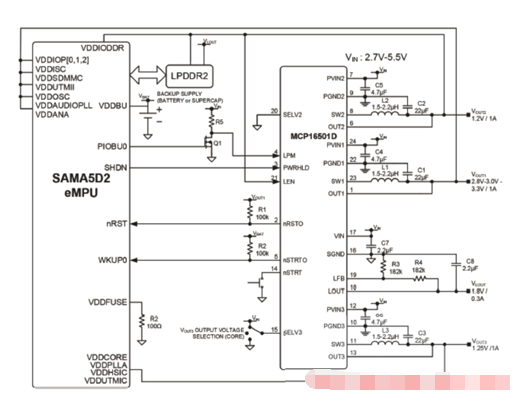
图2. MCP16501典型应用电路
评估板MIC28516
The MIC28516 Evaluation Board is a constant frequency, synchronous buck controller
featuring a unique adaptive on-time control architecture. The MIC28516 device
operates over an input supply range of 4.5V to 70V. The output voltage is adjustable
down to 0.6V with an ensured accuracy of ±1%. The device operates with a
programmable switching frequency from 270 kHz to 800 kHz.
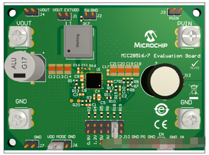
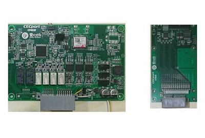
图3. 评估板MIC28516外形图
评估板MIC28516主要特性:
The MIC28516 Evaluation Board:
• Features a Soft Start (SS) time selection pin, which allows the user to adjust the
output Soft Start time to reduce inrush current from mains during start-up.
• Features six selectable output voltages: 0.8V, 1.2V, 2.5V, 3.3V, 5V and 12V.
• Features an auxiliary bootstrap Low Dropout (LDO) which improves the system
efficiency by supplying the internal bias power from the output of the converter.
• Features a logic level Enable (EN) signal that can be used to enable or disable the
controller.
• Can start up monotonically into a pre-biased output.
• Features an open-drain Power Good signal (PG), which signals when the output is in regulation.
The basic parameters of the evaluation board are:
• Input: 10V to 70V (optimized for 48V)
• Output: 0.8V, 1.2V, 2.5V, 3.3V, 5V or 12V Selectable through jumper J10 at 8A (default option is set to 5V)
• 270 kHz Switching Frequency (adjustable from 270 kHz to 800 kHz)
The MIC28516 Evaluation Board includes the following items:
• MIC28516 Evaluation Board (ADM00929)
• Important Information Sheet
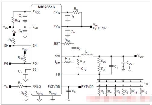
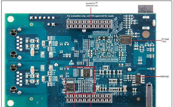
图4. 评估板MIC28516电路描述图
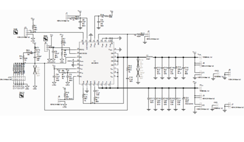
图5. 评估板MIC28516电路图
责任编辑:David
【免责声明】
1、本文内容、数据、图表等来源于网络引用或其他公开资料,版权归属原作者、原发表出处。若版权所有方对本文的引用持有异议,请联系拍明芯城(marketing@iczoom.com),本方将及时处理。
2、本文的引用仅供读者交流学习使用,不涉及商业目的。
3、本文内容仅代表作者观点,拍明芯城不对内容的准确性、可靠性或完整性提供明示或暗示的保证。读者阅读本文后做出的决定或行为,是基于自主意愿和独立判断做出的,请读者明确相关结果。
4、如需转载本方拥有版权的文章,请联系拍明芯城(marketing@iczoom.com)注明“转载原因”。未经允许私自转载拍明芯城将保留追究其法律责任的权利。
拍明芯城拥有对此声明的最终解释权。


 产品分类
产品分类




 2012- 2022 拍明芯城ICZOOM.com 版权所有 客服热线:400-693-8369 (9:00-18:00)


